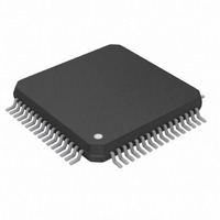
MAX3885ECB+D Maxim Integrated Products, MAX3885ECB+D Datasheet - Page 2

MAX3885ECB+D
Manufacturer Part Number
MAX3885ECB+D
Description
IC 1:16 DESERIALIZER 64-TQFP
Manufacturer
Maxim Integrated Products
Datasheet
1.MAX3885ECBD.pdf
(8 pages)
Specifications of MAX3885ECB+D
Function
Deserializer
Data Rate
2.5Gbps
Input Type
PECL
Output Type
LVDS
Number Of Inputs
1
Number Of Outputs
16
Voltage - Supply
3 V ~ 3.6 V
Operating Temperature
-40°C ~ 85°C
Mounting Type
Surface Mount
Package / Case
64-LQFP
Lead Free Status / RoHS Status
Lead free / RoHS Compliant
ABSOLUTE MAXIMUM RATINGS
Positive Supply Voltage (V
Input Voltage Level (all inputs)...................-0.5V to (V
Output Current LVDS outputs .............................................10mA
Continuous Power Dissipation (T
+3.3V, 2.488Gbps, SDH/SONET
1:16 Deserializer with LVDS Outputs
DC ELECTRICAL CHARACTERISTICS
(V
T
Stresses beyond those listed under “Absolute Maximum Ratings” may cause permanent damage to the device. These are stress ratings only, and functional
operation of the device at these or any other conditions beyond those indicated in the operational sections of the specifications is not implied. Exposure to
absolute maximum rating conditions for extended periods may affect device reliability.
AC ELECTRICAL CHARACTERISTICS
(V
T
Note 1: AC Characteristics guaranteed by design and characterization.
2
PECL INPUTS (SD+/-, SCLK+/-)
LVDS INPUTS AND OUTPUTS (SYNC+/-, PCLK+/-, PD_+/-)
A
Supply Current
Input High Voltage
Input Low Voltage
Input High Current
Input Low Current
Input Voltage Range
Differential Input Threshold
Threshold Hysteresis
Differential Input Resistance
Output High Voltage
Output Low Voltage
Differential Output Voltage
Change in Magnitude of Differential
Output Voltage for Complementary
States
Output Offset Voltage
Change in Magnitude of Output
Offset Voltage for Complementary
States
Single-Ended Output Resistance
Change in Magnitude of Single-
Ended Output Resistance for
Complementary Outputs
A
Maximum Serial Clock Frequency
Serial Data Setup Time
Serial Data Hold Time
Parallel Clock-to-Data Output Delay
TQFP (derate 24mW/°C above +85°C) .......................1000mW
CC
CC
= +25°C.)
= +25°C.) (Note 1, Figure 4)
_______________________________________________________________________________________
= +3.0V to +3.6V, differential loads = 100Ω ±1%, T
= +3.0V to +3.6V, differential loads = 100Ω ±1%, T
PARAMETER
PARAMETER
CC
)...............................-0.5V to +7.0V
A
= +85°C)
SYMBOL
SYMBOL
Δ ⎥ V
⎥ V
t
V
V
ΔV
f
CLK-Q
V
ΔR
SCLK
V
V
HYST
V
R
t
I
V
IDTH
R
I
I
V
SU
t
CC
IH
OH
OS
IL
OL
OD
H
IH
IN
IL
O
OD
OS
I
O
⎥
⎥
V
V
Differential input voltage = 100mV
Common-mode voltage = 50mV
Figure 1
CC
IN
IN
A
A
+ 0.5V)
= V
= V
= -40°C to +85°C, unless otherwise noted. Typical values are at V
= -40°C to +85°C, unless otherwise noted. Typical values are at V
IH(MAX)
IL(MIN)
CONDITIONS
CONDITIONS
Operating Temperature Range ...........................-40°C to +85°C
Storage Temperature Range .............................-60°C to +160°C
Lead Temperature (soldering, 10sec) .............................+300°C
V
V
CC
CC
0.925
1.125
2.488
-900
-900
-100
MIN
MIN
250
100
100
200
85
40
0
- 1.16
- 1.81
TYP
±2.5
TYP
200
100
450
78
95
V
V
CC
CC
1.475
1.275
MAX
MAX
280
900
900
100
115
400
±25
±25
140
±10
900
2.4
- 0.88
- 1.48
CC
CC
= +3.3V,
= +3.3V,
UNITS
UNITS
GHz
mA
mV
mV
mV
mV
mV
µA
µA
ps
ps
ps
%
Ω
Ω
V
V
V
V
V
V


