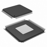
SCAN25100TYA/NOPB National Semiconductor, SCAN25100TYA/NOPB Datasheet - Page 16

SCAN25100TYA/NOPB
Manufacturer Part Number
SCAN25100TYA/NOPB
Description
IC SERIAL/DESERIAL CPRI 100-TQFP
Manufacturer
National Semiconductor
Series
SCANr
Datasheet
1.SCAN25100TYANOPB.pdf
(34 pages)
Specifications of SCAN25100TYA/NOPB
Function
Serializer/Deserializer
Data Rate
2.5Gbps
Input Type
LVTTL/LVCMOS
Output Type
LVTTL, LVCMOS
Number Of Inputs
10
Number Of Outputs
10
Voltage - Supply
1.7 V ~ 1.9 V
Operating Temperature
-40°C ~ 85°C
Mounting Type
Surface Mount
Package / Case
100-TQFP Exposed Pad, 100-eTQFP, 100-HTQFP, 100-VQFP
Operating Temperature (min)
-40C
Operating Temperature Classification
Industrial
Operating Temperature (max)
85C
Package Type
TQFP EP
Rad Hardened
No
Lead Free Status / RoHS Status
Lead free / RoHS Compliant
Other names
SCAN25100TYA
Available stocks
Company
Part Number
Manufacturer
Quantity
Price
Company:
Part Number:
SCAN25100TYA/NOPB
Manufacturer:
NS
Quantity:
158
Company:
Part Number:
SCAN25100TYA/NOPB
Manufacturer:
Texas Instruments
Quantity:
10 000
www.national.com
TRANSMIT DATA
DIN[9:0] Transmit Parallel Input Data
Transmit input data pins DIN[9:0] are latched on both rising
and falling edges of TXCLK. By using both TXCLK edges, the
Transmit Serial Data Output
DOUT is a differential current mode logic (CML) driver. Both
DOUTP and DOUTN are terminated with on-chip resistors to
an internal bias voltage. The values of the internal termination
resistors are controlled to 50Ω ±20%.
Transmitter Reset Options
RECEIVE DATAPATH
Receive Serial Data Input
The receive input (RIN) pins are terminated with on-chip
50Ω ±20% resistors to an internal bias voltage. This bias volt-
DIN[0]
DIN[1]
DIN[2]
DIN[3]
DIN[4]
DIN[5]
DIN[6]
DIN[7]
DIN[8]
DIN[9]
0
0
1
1
PE[1]
Tx Input
TXPWDNB
0
1
0
1
0
1
1
1
1
1
1
1
PE[0]
Coded Data Bit
Coded Data Bit
Coded Data Bit
Coded Data Bit
Coded Data Bit
Coded Data Bit
Coded Data Bit
Coded Data Bit
Coded Data Bit
Coded Data Bit
Missing REFCLK
Missing TXCLK
De-emphasis disabled.
De-emphasis enabled low (approximately 1 dB).
De-emphasis enabled medium (approximately 3 dB).
De-emphasis enabled high (approximately 6 dB).
10-bit Mode (TENBMODE = 1)
Not Locked
Not Locked
Tx PLL
Locked
Locked
Locked
X
TABLE 7. Transmit De-Emphasis Control Settings
TABLE 6. Transmitter Parallel Input Bus Mapping
TABLE 8. Transmitter Output Truth Table
Valid Dx.y or Kx.y
Invalid Kx.y
DIN[9:0]
x
x
x
x
x
x
16
clock speed is halved, which reduces high speed design and
EMI issues. The transmitter serializes and sends the valid
Dx.y or Kx.y code. If an invalid Kx.y code is provided at DIN
[9:0], the transmitter sends a K30.7 pattern.
Transmitter De-Emphasis
The transmitter serial output provides 3 steps of de-emphasis
to compensate for backplanes and cable interconnects.
Pulling both PE[1:0] pins low enables MDIO control of de-
emphasis.
age is set to approximately 1.45 volts above GND. Normally
CML signals are AC-coupled and this bias voltage sets the
input common mode for the RIN inputs. DC coupling between
two SCAN25100 devices is acceptable when required in the
application. For other CML outputs AC coupling is required.
Underflow / Overflow
Underflow / Overflow
Descriptions
Data Bit 0 (A, lsb)
Data Bit 1 (B)
Data Bit 2 (C)
Data Bit 3 (D)
Data Bit 4 (E)
Data Bit 5 (F)
Data Bit 6 (G)
Data Bit 7 (H, msb)
D/K Select (Z)
Pulled low through a 5 kΩ resistor
Tx FIFO
8-bit Mode (TENBMODE = 0)
Serial Data (10-bit Mode)
pulled to internal bias
pulled to internal bias
K30.7 (8-bit Mode) or
DOUTP and DOUTN
DOUTP and DOUTN
10'd0 (10-bit Mode)
Normal Serial Data
K30.7 (8-bit Mode)
DOUTP/DOUTN
Undefined
Logic 1


