DS92LV18TVV/NOPB National Semiconductor, DS92LV18TVV/NOPB Datasheet - Page 16
DS92LV18TVV/NOPB
Manufacturer Part Number
DS92LV18TVV/NOPB
Description
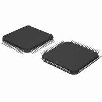
IC SER/DES LVDS 18BIT BUS 80LQFP
Manufacturer
National Semiconductor
Datasheet
1.DS92LV18TVVNOPB.pdf
(20 pages)
Specifications of DS92LV18TVV/NOPB
Function
Serializer/Deserializer
Data Rate
2.38Gbps
Input Type
LVTTL/LVCMOS
Output Type
LVTTL, LVCMOS
Number Of Inputs
18
Number Of Outputs
1
Voltage - Supply
3.15 V ~ 3.45 V
Operating Temperature
-40°C ~ 85°C
Mounting Type
Surface Mount
Package / Case
80-LQFP
No. Of Inputs
18
No. Of Outputs
18
Supply Voltage Range
3.15V To 3.45V
Driver Case Style
LQFP
No. Of Pins
80
Msl
MSL 3 - 168 Hours
Termination Type
SMD
Rohs Compliant
Yes
Filter Terminals
SMD
Digital Ic Case Style
LQFP
For Use With
LVDS-18B-EVK - BOARD EVALUATION DS92LV18
Lead Free Status / RoHS Status
Lead free / RoHS Compliant
Other names
*DS92LV18TVV
*DS92LV18TVV/NOPB
DS92LV18TVV
*DS92LV18TVV/NOPB
DS92LV18TVV
Available stocks
Company
Part Number
Manufacturer
Quantity
Price
Company:

Part Number:
DS92LV18TVV/NOPB
Manufacturer:
TI
Quantity:
1 000
Company:
Part Number:
DS92LV18TVV/NOPB
Manufacturer:
TI
Quantity:
2 170
Company:
Part Number:
DS92LV18TVV/NOPB
Manufacturer:
Texas Instruments
Quantity:
10 000
Part Number:
DS92LV18TVV/NOPB
Manufacturer:
NS/国半
Quantity:
20 000


www.national.com
Application Information
PVDD = PLL SECTION POWER SUPPLY
The PVDD pin supplies the PLL circuit. Note that the
DS92LV18 has two separate PLL and supply pins. The
PLL(s) require clean power for the minimization of Jitter. A
supply noise frequency in the 300 kHz to 1 MHz range can
cause increased output jitter. Certain power supplies may
have switching frequencies or high harmonic content in this
range. If this is the case, filtering of this noise spectrum may
be required. A notch filter response is best to provide a stable
VDD, suppression of the noise band, and good high-
frequency response (clock fundamental). This may be ac-
complished with a pie filter (CRC or CLC). If employed, a
separate pie filter is recommended for each PLL to minimize
drop in potential due to the series resistance. The pie filter
should be located close to the PVDD power pin. Separate
power planes for the PVDD pins is typically not required.
AVDD = LVDS SECTION POWER SUPPLY
The AVDD pins power the LVDS portion of the circuit. The
DS92LV18 has four AVDD pins. Due to the nature of the
design, current draw is not excessive on these pins. A 0.1uF
Truth Tables
RPWDN (Pin 01)
TPWDN (Pin 42)
H
H
H
L
H
H
H
L
REN (Pin 02)
X
H
H
L
DEN (Pin 19)
H
H
X
L
RX PLL Status (Internal)
(Continued)
Not Locked
Locked
Transmitter Truth Table
X
X
TX PLL Status (Internal)
Receiver Truth Table
Not Locked
Locked
16
X
X
ROUTn & RCLK (See Pin Diagram)
capacitor is sufficient for these pins. If space is available, a
0.01uF capacitor may be used in parallel with the 0.1uF
capacitor for additional high frequency filtering.
GROUNDS
The AGND pin should be connected to the signal common in
the cable for the return path of any common-mode current.
Most of the LVDS current will be odd-mode and return within
the interconnect pair. A small amount of current may be
even-mode due to coupled noise and driver imbalances.
This current should return via a low impedance known path.
A solid ground plane is recommended for both DVDD, PVDD
or AVDD. Using a split plane may cause ground loops or a
difference in ground potential at various ground pins of the
device.
Data & CLK Active
Hi Z
Hi Z
H
Serialized Data with Embedded Clock
LVDS Outputs (Pins 13 and 14)
Hi Z
Hi Z
Hi Z
H = PLL Unlocked
L = PLL Locked;
LOCK (Pin 63)
Hi Z
H
L
Related parts for DS92LV18TVV/NOPB
Image
Part Number
Description
Manufacturer
Datasheet
Request
R

Part Number:
Description:
National Semiconductor [8-Bit D/A Converter]
Manufacturer:
National Semiconductor
Datasheet:
Part Number:
Description:
National Semiconductor [Media Coprocessor]
Manufacturer:
National Semiconductor
Datasheet:
Part Number:
Description:
Digitally Controlled Tone and Volume Circuit with Stereo Audio Power Amplifier, Microphone Preamp Stage and National 3D Sound
Manufacturer:
National Semiconductor
Datasheet:
Part Number:
Description:
Digitally Controlled Tone and Volume Circuit with Stereo Audio Power Amplifier, Microphone Preamp Stage and National 3D Sound
Manufacturer:
National Semiconductor
Datasheet:
Part Number:
Description:
AC97 Rev 2 Codec with Sample Rate Conversion and National 3D Sound
Manufacturer:
National Semiconductor
Part Number:
Description:
Manufacturer:
National Semiconductor
Datasheet:
Part Number:
Description:
Manufacturer:
National Semiconductor
Datasheet:
Part Number:
Description:
General Purpose, Low Voltage, Low Power, Rail-to-Rail Output Operational Amplifiers
Manufacturer:
National Semiconductor
Datasheet:
Part Number:
Description:
8-bit 20 MSPS flash A/D converter.
Manufacturer:
National Semiconductor
Datasheet:
Part Number:
Description:
Low Noise Quad Operational Amplifier
Manufacturer:
National Semiconductor
Datasheet:
Part Number:
Description:
Quad Differential Line Receivers
Manufacturer:
National Semiconductor
Datasheet:
Part Number:
Description:
Quad High Speed Trapezoidal? Bus Transceiver
Manufacturer:
National Semiconductor
Datasheet:
Part Number:
Description:
Dual Line Receiver
Manufacturer:
National Semiconductor
Datasheet:
Part Number:
Description:
TTL to 10k ECL Level Translator with Latch
Manufacturer:
National Semiconductor
Datasheet: