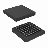
SCAN921226HSM/NOPB National Semiconductor, SCAN921226HSM/NOPB Datasheet - Page 7

SCAN921226HSM/NOPB
Manufacturer Part Number
SCAN921226HSM/NOPB
Description
IC SER/DESER HI TEMP 80MHZ LVDS
Manufacturer
National Semiconductor
Series
SCANr
Datasheet
1.SCAN921025HSMNOPB.pdf
(21 pages)
Specifications of SCAN921226HSM/NOPB
Function
Deserializer
Data Rate
800Mbps
Input Type
LVDS
Output Type
LVDS
Number Of Inputs
1
Number Of Outputs
10
Voltage - Supply
3 V ~ 3.6 V
Operating Temperature
-40°C ~ 125°C
Mounting Type
Surface Mount
Package / Case
49-FBGA
Lead Free Status / RoHS Status
Lead free / RoHS Compliant
Other names
*SCAN921226HSM
*SCAN921226HSM/NOPB
SCAN921226HSM
*SCAN921226HSM/NOPB
SCAN921226HSM
Available stocks
Company
Part Number
Manufacturer
Quantity
Price
Company:
Part Number:
SCAN921226HSM/NOPB
Manufacturer:
NSC
Quantity:
964
Symbol
t
t
t
t
t
t
t
t
t
t
t
t
t
t
t
t
t
t
t
t
t
t
t
Symbol
DIS
DIH
HZD
LZD
ZHD
ZLD
SPW
PLD
SD
DJIT
RJIT
RFCP
RFDC
RFCP
TCP
RFTT
RCP
CLH
CHL
DD
ROS
ROH
RDC
Symbol
Serializer Switching Characteristics
Over recommended operating supply and temperature ranges unless otherwise specified.
Deserializer Timing Requirements for REFCLK
Over recommended operating supply and temperature ranges unless otherwise specified.
Deserializer Switching Characteristics
Over recommended operating supply and temperature ranges unless otherwise specified.
/
Receiver out Clock
Period
CMOS/TTL
Low-to-High Transition
Time
CMOS/TTL
High-to-Low Transition
Time
Deserializer Delay
Figure 12
ROUT Data Valid
before RCLK
ROUT Data Valid after
RCLK
RCLK Duty Cycle
DIN (0-9) Setup to TCLK R
DIN (0-9) Hold from
TCLK
DO
TRI-STATE Delay
DO
TRI-STATE Delay
DO
HIGH Delay
DO
LOW Delay
SYNC Pulse Width
Serializer PLL Lock Time
Serializer Delay
Deterministic Jitter
Random Jitter
REFCLK Period
REFCLK Duty Cycle
Ratio of REFCLK to
TCLK
REFCLK Transition Time
±
±
±
±
Parameter
HIGH to
LOW to
TRI-STATE to
TRI-STATE to
Parameter
Parameter
t
Figure 11
CL = 15 pF
Figure 5
Figure 13
Figure 13
RCP
Room Temp, 3.3V
Room Temp, 3.3V
All Temp, All Freq
C
Figure 7
R
C
Figure 8
(Note 5)
R
Figure 10
R
Conditions
= t
L
L
L
L
L
L
=10pF to GND
=10pF to GND
= 27Ω,
= 27Ω,
= 27Ω
= 27Ω, Figure 11
TCP
R
C
to GND,
(Note 6)
L
L
=10pF
= 27Ω,
Conditions
Conditions
Rout(0-9),
Pin/Freq.
20MHz
80MHz
20MHz
80MHz
20MHz
80MHz
LOCK,
RCLK
RCLK
RCLK
RCLK
20MHz
80MHz
(Continued)
7
1.75*t
1.75*t
1.75*t
-0.35*t
0.35*t
-0.4*t
0.4*t
12.5
t
Min
510*t
TCP
30
95
12.5
Min
5*t
RCP
RCP
RCP
45
-330
-130
Min
4.0
RCP
0
TCP
+ 1.0
RCP
RCP
RCP
+1.25
+2.25
+2.25
TCP
1.75*t
1.75*t
1.75*t
t
-0.5*t
-0.5*t
TCP
0.5*t
0.5*t
Typ
50
Typ
T
1
3
6.5
-40
Typ
1.2
1.1
50
RCP
RCP
RCP
3
3
5
6
+ 2.5
RCP
RCP
RCP
RCP
+5.0
+5.0
+5.0
1.75*t
1.75*t
1.75*t
t
513*t
TCP
Max
140
+60
Max
50.0
105
10
10
10
10
10
70
+ 3.5
Max
50.0
6
55
RCP
RCP
RCP
TCP
4
4
+8.5
+8.0
+8.0
www.national.com
ps (RMS)
Units
Units
Units
ns
ns
ns
ns
ns
ns
ns
ns
ns
ps
ps
ns
ns
%
ns
ns
ns
ns
ns
ns
ns
ns
ns
ns
%


