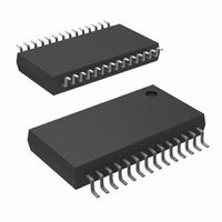
DS92LV1224TMSA/NOPB National Semiconductor, DS92LV1224TMSA/NOPB Datasheet - Page 6

DS92LV1224TMSA/NOPB
Manufacturer Part Number
DS92LV1224TMSA/NOPB
Description
IC DESERIALIZER 10-BIT 28-SSOP
Manufacturer
National Semiconductor
Datasheet
1.DS92LV1224TMSANOPB.pdf
(13 pages)
Specifications of DS92LV1224TMSA/NOPB
Function
Deserializer
Data Rate
660Mbps
Input Type
LVDS
Output Type
LVTTL
Number Of Inputs
1
Number Of Outputs
10
Voltage - Supply
3 V ~ 3.6 V
Operating Temperature
-40°C ~ 85°C
Mounting Type
Surface Mount
Package / Case
28-SSOP
Lead Free Status / RoHS Status
Lead free / RoHS Compliant
Other names
*DS92LV1224TMSA
*DS92LV1224TMSA/NOPB
DS92LV1224TMSA
*DS92LV1224TMSA/NOPB
DS92LV1224TMSA
www.national.com
t
t
t
t
t
t
t
t
t
t
t
t
t
t
t
t
t
t
Symbol
TCP
TCIH
TCIL
CLKT
JIT
LLHT
LHLT
DIS
DIH
HZD
LZD
ZHD
ZLD
SPW
PLD
SD
DJIT
RJIT
Symbol
Serializer Timing Requirements for TCLK
Over recommended operating supply and temperature ranges unless otherwise specified.
Serializer Switching Characteristics
Over recommended operating supply and temperature ranges unless otherwise specified.
Note 1: “Absolute Maximum Ratings” are those values beyond which the
safety of the device cannot be guaranteed. They are not meant to imply that
the devices should be operated at these limits. The table of “Electrical
Characteristics” specifies conditions of device operation.
Note 2: Typical values are given for V
Note 3: Current into device pins is defined as positive. Current out of device
pins is defined as negative. Voltages are referenced to ground except VOD,
∆VOD, VTH and VTL which are differential voltages.
Bus LVDS Low-to-High
Transition Time
Bus LVDS High-to-Low
Transition Time
DIN (0-9) Setup to TCLK
DIN (0-9) Hold from TCLK
DO
TRI-STATE Delay
DO
Delay
DO
HIGH Delay
DO
Delay
SYNC Pulse Width
Serializer PLL Lock Time
Serializer Delay
Deterministic Jitter
Random Jitter
Transmit Clock Period
Transmit Clock High Time
Transmit Clock Low Time
TCLK Input Transition
Time
TCLK Input Jitter
±
±
±
±
HIGH to
LOW to TRI-STATE
TRI-STATE to
TRI-STATE to LOW
Parameter
Parameter
CC
= 3.3V and T
R
C
Figure 3
(Note 4)
R
C
Figure 5
R
C
Figure 6
(Note 5)
R
Figure 8
R
L
L
L
L
L
L
L
L
=10pF to GND
=10pF to GND
=10pF to GND
= 27Ω
= 27Ω,
= 27Ω,
= 27Ω
= 27Ω, Figure 9
R
C
C
to GND,
(Note 6)
L
L
L
=10pF to GND
Conditions
A
Conditions
=10pF
= 27Ω,
R
= +25˚C.
L
= 27Ω,
MHz
MHz
40
66
6
Note 4: t
using statistical analysis.
Note 5: Because the Serializer is in TRI-STATE mode, the Deserializer will
lose PLL lock and have to resynchronize before data transfer.
Note 6: t
analysis.
t
510*t
TCP
15.15
0.4T
0.4T
5*t
Min
-320
-200
Min
4.0
0
+ 1.0
TCP
TCP
LLHT
DJIT
specifications are Guranteed By Design using statistical
and t
LHLT
t
TCP
specifications are Guranteed By Design (GBD)
0.5T
0.5T
0.25
Typ
Typ
0.2
6.5
-80
-70
19
T
3
3
5
3
+ 2.0
t
513*t
TCP
Max
150
0.4
0.4
0.6T
0.6T
10
10
10
10
80
25
Max
25.0
150
+ 3.0
6
TCP
pS (RMS)
Units
(RMS)
Units
nS
nS
nS
nS
nS
nS
nS
nS
nS
nS
nS
pS
pS
nS
nS
nS
nS
pS


