LM2506GR/NOPB National Semiconductor, LM2506GR/NOPB Datasheet
LM2506GR/NOPB
Specifications of LM2506GR/NOPB
Available stocks


Related parts for LM2506GR/NOPB

LM2506GR/NOPB Summary of contents
Page 1
... SER (PD The LM2506 implements the physical layer of the MPL Level 0 Standard (MPL-0) and a 150 µ Typical Application Diagram - Bridge Chips © 2006 National Semiconductor Corporation Features n RGB Display Interface support up to 800 x 300 n MPL-Level 0 Physical Layer using two data and one ...
Page 2
Typical Application Diagram - RGB Mode to Display Driver Ordering Information NSID LM2506GR LM2506SQ www.national.com Package Type 49L MicroArray, 4.0 X 4.0 X 1.0 mm, 0.5 mm pitch 40L LLP, 5.0 X 5.0 X 0.8 mm, 0.4 mm pitch 2 ...
Page 3
Pin Descriptions - RGB Mode No. Pin Name I/O, Type of Pins MPL SERIAL BUS PINS MD[1:0] 2 IO, MPL MC 1 IO, MPL V Ground SSA CONFIGURATION/PARALLEL BUS PINS RGB LVCMOS M/ LVCMOS TM 1 ...
Page 4
... Absolute Maximum Ratings If Military/Aerospace specified devices are required, please contact the National Semiconductor Sales Office/ Distributors for availability and specifications. Supply Voltage (V ) DDA Supply Voltage ( Supply Voltage (V ) DDIO LVCMOS Input/Output Voltage MPL Input/Output Voltage Junction Temperature Storage Temperature Lead Temperature Soldering, ...
Page 5
Electrical Characteristics Over recommended operating supply and temperature ranges unless otherwise specified. (Notes 2, 3) Symbol Parameter MPL I Supply Current — Disable DDZ T = 25˚C A Power Down Modes PD Power Dissipation Switching Characteristics Over recommended operating supply ...
Page 6
Recommended Input Timing Requirements Over recommended operating supply and temperature ranges unless otherwise specified. (Note 2) Symbol Parameter SER PIXEL CLOCK (PCLK) f Pixel Clock Frequency t Pixel Clock Period CP PCLK Pixel Clock Duty Cycle DC t Transition Time ...
Page 7
Timing Diagrams (Continued) Functional Description BUS OVERVIEW The LM2506 is a dual link SER/DES configurable part that supports an 18-bit RGB Display interface. The MPL physical layer is purpose-built for an extremely low power and low EMI data transmission while ...
Page 8
Functional Description The MPL start up sequence gives the DES an opportunity to optimize the current sources in its receivers to maximize noise margins. The SER begins the sequence by driving the MC line logically Low for 180 MC cycles ...
Page 9
Functional Description Pixel bandwidth is equal to display resolution times color depth times frame rate. Net Bandwidth = (Pixel BW)(24/18)(1 Blanking) Net bandwidth is equal to the pixel bandwidth times the overhead times the blanking overhead. Format Hor. ...
Page 10
Functional Description uses two bits that are already required in the 6-MC cycle transaction. Since double-edge clocking is used with two data signals, adding one clock cycle to the transaction actu- ally adds four bits. One of these bits is ...
Page 11
Functional Description TABLE 2. Serializer Input Timing Parameters for RGB Interface Sym. t Data (RGB, DE HS) to PCLK - Set Time SET t PCLK to Data (RGB, DE HS) - Hold Time HOLD Note 10: ...
Page 12
LM2506 Features and Operation POWER SUPPLIES The V and V (MPL and PLL) must be connected to DDcore DDA the same potential between 1.74V and 2.0V. V the logic interface and may be powered between 1.74 and 3. ...
Page 13
LM2506 Features and Operation Application Information SYSTEM CONSIDERATIONS When employing the MPL SER/DES chipset in place of a parallel bus, a few system considerations must be taken into account. VDDIO levels of the Host and SER must be com- patible. ...
Page 14
Application Information Power and Ground - Bumped Package Power and ground bump assignments are shown in Figure 15. The nine center balls must be connected ground on the FIGURE 15. LM2506 PWR (V FLEX CIRCUIT RECOMMENDATIONS The three MPL lines ...
Page 15
Application Information (Continued) FIGURE 16. MPL Interface Layout 15 20125562 www.national.com ...
Page 16
Connection Diagram microArray Package RGB SER Pinout SER PCLK DDIO RGB DES Pinout DES DDIO E B4 ...
Page 17
Connection Diagram - LLP Package Pin # SER MD1 MD0 PDOUT PCLK DAP Note: ...
Page 18
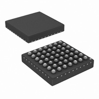
Physical Dimensions www.national.com inches (millimeters) unless otherwise noted 49L MicroArray, 0.5mm pitch Order Number LM2506GR NS Package Number GRA49A 40L LLP, 0.4mm pitch Order Number LM2506SQ NS Package Number SQF40A 18 ...
Page 19
... BANNED SUBSTANCE COMPLIANCE National Semiconductor follows the provisions of the Product Stewardship Guide for Customers (CSP-9-111C2) and Banned Substances and Materials of Interest Specification (CSP-9-111S2) for regulatory environmental compliance. Details may be found at: www.national.com/quality/green. ...