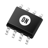
NCV1124DR2G ON Semiconductor, NCV1124DR2G Datasheet - Page 4

NCV1124DR2G
Manufacturer Part Number
NCV1124DR2G
Description
IC SENSOR DUAL VAR-RELUCT 8-SOIC
Manufacturer
ON Semiconductor
Type
Variable Reluctancer
Datasheet
1.NCV1124DG.pdf
(8 pages)
Specifications of NCV1124DR2G
Input Type
Logic
Output Type
Logic
Interface
Dual, Serial or Parallel
Current - Supply
5mA
Mounting Type
Surface Mount
Package / Case
8-SOIC (3.9mm Width)
Mounting Style
SMD/SMT
Lead Free Status / RoHS Status
Lead free / RoHS Compliant
Available stocks
Company
Part Number
Manufacturer
Quantity
Price
Company:
Part Number:
NCV1124DR2G
Manufacturer:
ON Semiconductor
Quantity:
8 750
Part Number:
NCV1124DR2G
Manufacturer:
ON/安森美
Quantity:
20 000
the necessary external components. Both channels share the
IN
description of the components is as follows:
− amplitude usually increases with frequency, depending on
loading.
biasing.
points via R1/R
set at 160 mV.
frequency as V
COMP1 with V
the DC biased voltage at V
condition is needed when crossing in the positive direction,
(V
crossing in the negative direction,
therefore,
V RS(+TRP) t IN Adj
V RS(−TRP) t IN Adj
INP1(R1 ) R RS ) ) V RS u IN Adj
Figure 2 shows one channel of the NCV1124 along with
V
R
R1/R
INP1/IN
COMP1 − Internal comparator with built−in hysteresis
OUT1 − Output 0 V − 5.0 V square wave with the same
By inspection, the voltage at the (+) and (−) terminals of
As V
To get comparator COMP1 to trip, the following
Combining equations 2, 3, and 4, we get:
It should be evident that tripping on the negative side is:
In normal mode,
Adj
HYS
RS
RS
pin as the negative input to a comparator. A brief
− Ideal sinusoidal, ground referenced, sensor output
− Source impedance of sensor.
RS
is the built−in hysteresis set to 160 mV), or when
Adj
begins to rise and fall, it will be superimposed on
Adj
− External resistors for current limiting and
V + + INP1(R1 ) R RS ) ) V RS
− Internal current sources that determine trip
RS
Adj
RS
NORMAL OPERATION
V + + INP1(R1 ) R RS )
.
.
= 0V are:
V − + IN Adj
V + u V − ) V HYS
V + t V − * V HYS
R Adj * INP1(R1 ) R RS ) ) V HYS
R Adj * INP1(R1 ) R RS ) * V HYS
+
.
R Adj
R Adj ) V HYS
THEORY OF OPERATION
http://onsemi.com
(1)
(2)
(3)
(4)
(5)
(6)
(7)
(8)
NCV1124
4
you can detect signals with as little amplitude as V
V), will increase the IN
needed to trip comparator COMP1. However, if no V
signal is present, then we can use equations 1, 2, and 4
(equation 5 does not apply in this mode) to get:
Since R
R
when entering the diag mode with V
impedance must be greater than the above calculated value.
This can be very useful in diagnosing intermittent sensor.
input to limit the voltage on the input pin and prevent
substrate current injection. The clamp is specified to handle
±12 mA. This puts an upper limit on the amplitude of the
sensor output. For example, if R1 = 20 k, then
MHz if the input signal does not activate the positive or
negative input clamps. Frequency performance will be
lower when the positive or negative clamps are active.
Typical performance will be up to a frequency of 680 kHz
with the clamps active.
RS
We can now re−write equation (7) as:
By making
A design example is given in the applications section.
The NCV1124 has a DIAG pin that when pulled high (5.0
Equation (7) shows that a larger V
Equation (13) shows that if the output switches states
As shown in Figure 2, an active clamp is provided on each
Therefore, the V
The NCV1124 will typically run at a frequency up to 1.8
,
V RS(+TR) u INP1(R Adj * R1 * R RS ) ) V HYS
INP1(R1 ) R RS ) u INP1
RS
R RS +
V RS(MAX) + 20 k
is the only unknown variable we can solve for
OPEN SENSOR PROTECTION
INP1
INPUT PROTECTION
RS(pk−pk)
R Adj + R1 ) R RS
INP1 + IN Adj
Adj
K I
current source by roughly 50%.
INP1
voltage can be as high as 480 V.
R Adj ) V HYS
12 mA + 240 V
K I
RS(+TRP)
RS
R Adj ) V HYS
= 0, the sensor
voltage will be
* R1
HYS
(10)
.
(12)
(13)
(11)
(9)
RS


