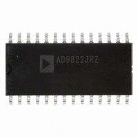
AD9822JRZ Analog Devices Inc, AD9822JRZ Datasheet - Page 8

AD9822JRZ
Manufacturer Part Number
AD9822JRZ
Description
IC CCD SIGNAL PROC 14BIT 28-SOIC
Manufacturer
Analog Devices Inc
Type
CCD Signal Processor, 14-Bitr
Datasheet
1.AD9822JRSZRL.pdf
(20 pages)
Specifications of AD9822JRZ
Input Type
Logic
Output Type
Logic
Interface
3-Wire Serial
Current - Supply
73mA
Mounting Type
Surface Mount
Package / Case
28-SOIC (7.5mm Width)
Analog Front End Type
CCD/CIS
Analog Front End Category
Video
Interface Type
Serial (3-Wire)
Sample Rate
15MSPS
Input Voltage Range
1V
Operating Supply Voltage (min)
3/4.75V
Operating Supply Voltage (typ)
5V
Operating Supply Voltage (max)
5.25V
Resolution
14b
Supply Current
4/73mA
Number Of Adc's
1
Power Supply Type
Analog/Digital
Operating Temp Range
0C to 70C
Operating Temperature Classification
Commercial
Mounting
Surface Mount
Pin Count
28
Package Type
SOIC W
Number Of Channels
3
Lead Free Status / RoHS Status
Lead free / RoHS Compliant
Available stocks
Company
Part Number
Manufacturer
Quantity
Price
Part Number:
AD9822JRZ
Manufacturer:
ADI/亚德诺
Quantity:
20 000
AD9822
TERMINOLOGY
Integral Nonlinearity (INL)
Integral nonlinearity error refers to the deviation of each
individual code from a line drawn from zero scale through
positive full scale. The point used as zero scale occurs ½ LSB
before the first code transition. Positive full scale is defined as a
level 1 ½ LSB beyond the last code transition. The deviation is
measured from the middle of each particular code to the true
straight line.
Differential Nonlinearity (DNL)
An ideal ADC exhibits code transitions that are exactly 1 LSB
apart. DNL is the deviation from this ideal value; therefore,
every code must have a finite width. No missing codes
guaranteed to 14-bit resolution indicates that all 16384 codes,
respectively, must be present over all operating ranges.
Offset Error
The first ADC code transition should occur at a level ½ LSB
above the nominal zero-scale voltage. The offset error is the
deviation of the actual first code transition level from the ideal
level.
Gain Error
The last code transition should occur for an analog value
1 ½ LSB below the nominal full-scale voltage. Gain error is the
deviation of the actual difference between the first and last code
transitions and the ideal difference between the first and last
code transitions.
Rev. B | Page 8 of 20
Input Referred Noise
The rms output noise is measured using histogram techniques.
The ADC output codes’ standard deviation is calculated in LSB
and converted to an equivalent voltage, using the relationship
1 LSB = 4 V/16384 = 244 mV. The noise is then referred to the
input of the AD9822 by dividing by the PGA gain.
Channel-to-Channel Crosstalk
In an ideal 3-channel system, the signal in one channel will not
influence the signal level of another channel. The channel-to-
channel crosstalk specification is a measure of the change that
occurs in one channel as the other two channels are varied. In
the AD9822, one channel is grounded and the other two
channels are exercised with full-scale input signals. The
change in the output codes from the first channel is measured
and compared with the result when all three channels are
grounded. The difference is the channel-to-channel crosstalk,
stated in LSB.
Aperture Delay
The time delay that occurs from when a sampling edge is
applied to the AD9822 until the actual sample of the input
signal is held. Both CDSCLK1 and CDSCLK2 sample the input
signal during the transition from high to low; therefore, the
aperture delay is measured from each clock’s falling edge to the
instant the actual internal sample is taken.
Power Supply Rejection
It specifies the maximum full-scale change that occurs from
the initial value when the supplies are varied over the
specified limits.


