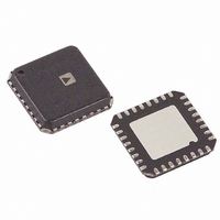
AD9944KCP Analog Devices Inc, AD9944KCP Datasheet - Page 8

AD9944KCP
Manufacturer Part Number
AD9944KCP
Description
IC CCD SIGNAL PROCESSOR 32-LFCSP
Manufacturer
Analog Devices Inc
Type
CCD Signal Processor, 12-Bitr
Datasheet
1.AD9943KCPZRL.pdf
(20 pages)
Specifications of AD9944KCP
Rohs Status
RoHS non-compliant
Input Type
Logic
Output Type
Logic
Interface
3-Wire Serial
Mounting Type
Surface Mount
Package / Case
32-LFCSP
Analog Front End Type
CCD
Analog Front End Category
Video
Interface Type
Serial (3-Wire)
Input Voltage Range
0.5V
Operating Supply Voltage (min)
2.7V
Operating Supply Voltage (typ)
3V
Operating Supply Voltage (max)
3.6V
Resolution
12b
Number Of Adc's
1
Power Supply Type
Analog/Digital
Operating Temp Range
-20C to 85C
Operating Temperature Classification
Commercial
Mounting
Surface Mount
Pin Count
32
Package Type
LFCSP EP
Number Of Channels
1
Current - Supply
-
Lead Free Status / RoHS Status
Not Compliant
Available stocks
Company
Part Number
Manufacturer
Quantity
Price
Company:
Part Number:
AD9944KCP
Manufacturer:
XILINX
Quantity:
2
Part Number:
AD9944KCP
Manufacturer:
ADI/亚德诺
Quantity:
20 000
Company:
Part Number:
AD9944KCPRL
Manufacturer:
INTEL
Quantity:
10
AD9943/AD9944
AD9943 PIN CONFIGURATION AND FUNCTION DESCRIPTIONS
Table 7. AD9943 Pin Function Descriptions
Pin No.
1 to 10
11
12
13
14
15
16
17
18
19
20
21
22
23
24
25
26
27
28 to 30
31 to 32
1
Type: AI = analog input, AO = analog output, DI = digital input, DO = digital output, P = power, and NC = no connect.
Mnemonic
D0 to D9
DRVDD
DRVSS
DVDD
DATACLK
DVSS
PBLK
CLPOB
SHP
SHD
AVDD
AVSS
CCDIN
REFT
REFB
SL
SDATA
SCK
NC
NC
Type
DO
P
P
P
DI
P
DI
DI
DI
DI
P
P
AI
AO
AO
DI
DI
DI
NC
NC
1
Description
Digital Data Outputs.
Digital Output Driver Supply.
Digital Output Driver Ground.
Digital Supply.
Digital Data Output Latch Clock.
Digital Supply Ground.
Preblanking Clock Input.
Black Level Clamp Clock Input.
CDS Sampling Clock for CCD Reference Level.
CDS Sampling Clock for CCD Data Level.
Analog Supply.
Analog Ground.
Analog Input for CCD Signal.
A/D Converter Top Reference Voltage Decoupling.
A/D Converter Bottom Reference Voltage Decoupling.
Serial Digital Interface Load Pulse.
Serial Digital Interface Data Input.
Serial Digital Interface Clock Input.
Internally pulled down. Float or connect to GND.
Internally not nonnected.
D0 1
D1 2
D2 3
D3 4
D4 5
D5 6
D6 7
D7 8
NC = NO CONNECT
Figure 2. AD9943 Pin Configuration
Rev. B | Page 8 of 20
PIN 1
INDICATOR
AD9943
TOP VIEW
24 REFB
23 REFT
22 CCDIN
21 AVSS
20 AVDD
19 SHD
18 SHP
17 CLPOB


