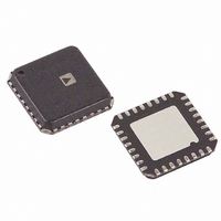
AD9943KCP Analog Devices Inc, AD9943KCP Datasheet - Page 18

AD9943KCP
Manufacturer Part Number
AD9943KCP
Description
IC CCD SIGNAL PROCESSOR 32-LFCSP
Manufacturer
Analog Devices Inc
Type
CCD Signal Processor, 10-Bitr
Datasheet
1.AD9943KCPZRL.pdf
(20 pages)
Specifications of AD9943KCP
Rohs Status
RoHS non-compliant
Input Type
Logic
Output Type
Logic
Interface
3-Wire Serial
Mounting Type
Surface Mount
Package / Case
32-LFCSP
Analog Front End Type
CCD
Analog Front End Category
Video
Interface Type
Serial (3-Wire)
Input Voltage Range
0.5V
Operating Supply Voltage (min)
2.7V
Operating Supply Voltage (typ)
3V
Operating Supply Voltage (max)
3.6V
Resolution
10b
Number Of Adc's
1
Power Supply Type
Analog/Digital
Operating Temp Range
-20C to 85C
Operating Temperature Classification
Commercial
Mounting
Surface Mount
Pin Count
32
Package Type
LFCSP EP
Number Of Channels
1
Current - Supply
-
Lead Free Status / RoHS Status
Not Compliant
Available stocks
Company
Part Number
Manufacturer
Quantity
Price
Company:
Part Number:
AD9943KCP
Manufacturer:
MOLEX
Quantity:
110
Company:
Part Number:
AD9943KCP
Manufacturer:
ADI
Quantity:
624
Company:
Part Number:
AD9943KCPZ
Manufacturer:
ADI
Quantity:
585
Part Number:
AD9943KCPZ
Manufacturer:
ADI/亚德诺
Quantity:
20 000
Company:
Part Number:
AD9943KCPZRL
Manufacturer:
SANYO
Quantity:
410
Company:
Part Number:
AD9943KCPZRL
Manufacturer:
ADI
Quantity:
15 000
AD9943/AD9944
APPLICATIONS INFORMATION
The AD9943/AD9944 are complete analog front end (AFE)
products for digital still camera and camcorder applications. As
shown in Figure 12, the CCD image (pixel) data is buffered and
sent to the AD9943/AD9944 analog input through a series input
capacitor. The AD9943/AD9944 perform the dc restoration,
CDS, gain adjustment, black level correction, and analog-to-
digital conversion. The AD9943/AD9944’s digital output data is
OUTPUTS
DATA
V-DRIVE
10
CCD
V
OUT
NC = NO CONNECT
D0
D1
D2
D3
D4
D5
D6
D7
Figure 17. AD9943 Recommended Circuit Configuration for CCD Mode
SUPPLY
BUFFER
DRIVER
1
2
3
4
5
6
7
8
INTERFACE
3V
32 31 30 29 28 27 26 25
9 10
SERIAL
0.1µF
Figure 16. System Applications Diagram
0.1µF
TIMING
PIN 1
IDENTIFIER
11
CCD
(Not to Scale)
TOP VIEW
12 13 14 15 16
AD9943
Rev. B | Page 18 of 20
CCDIN
AD9943/AD9944
3
GENERATOR
0.1µF
TIMING
REGISTER
CDS/CLAMP
TIMING
3V
ANALOG
SUPPLY
ADC
DATA
then processed by the image processing ASIC. The internal
registers of the AD9943/AD9944—used to control gain, offset
level, and other functions—are programmed by the ASIC or
microprocessor through a 3-wire serial digital interface. A
system timing generator provides the clock signals for both the
CCD and the AFE.
OUT
24
23
22
21
20
19
18
17
REFB
REFT
CCDIN
AVSS
AVDD
SHD
SHP
CLPOB
INTERFACE
OUTPUTS
DIGITAL
SERIAL
0.1µF
1.0µF
1.0µF
5
DIGITAL IMAGE
PROCESSING
ASIC
CLOCK
INPUTS
0.1µF
3V
ANALOG
SUPPLY
CCDIN


