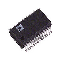
AD9822JRS Analog Devices Inc, AD9822JRS Datasheet - Page 16

AD9822JRS
Manufacturer Part Number
AD9822JRS
Description
IC CCD SIGNAL PROC 14BIT 28-SSOP
Manufacturer
Analog Devices Inc
Type
CCD Signal Processor, 14-Bitr
Datasheet
1.AD9822JRSZRL.pdf
(20 pages)
Specifications of AD9822JRS
Rohs Status
RoHS non-compliant
Input Type
Logic
Output Type
Logic
Interface
3-Wire Serial
Current - Supply
73mA
Mounting Type
Surface Mount
Package / Case
28-SSOP
Analog Front End Type
CCD/CIS
Analog Front End Category
Video
Interface Type
Serial (3-Wire)
Sample Rate
15MSPS
Input Voltage Range
1V
Operating Supply Voltage (min)
3/4.75V
Operating Supply Voltage (typ)
5V
Operating Supply Voltage (max)
5.25V
Resolution
14b
Supply Current
4/73mA
Number Of Adc's
1
Power Supply Type
Analog/Digital
Operating Temp Range
0C to 70C
Operating Temperature Classification
Commercial
Mounting
Surface Mount
Pin Count
28
Package Type
SSOP
Number Of Channels
3
Lead Free Status / RoHS Status
Not Compliant
Available stocks
Company
Part Number
Manufacturer
Quantity
Price
Company:
Part Number:
AD9822JRS
Manufacturer:
AD
Quantity:
1 551
Part Number:
AD9822JRS
Manufacturer:
ADI/亚德诺
Quantity:
20 000
Company:
Part Number:
AD9822JRSRL
Manufacturer:
RENESAS
Quantity:
442
Part Number:
AD9822JRSRL
Manufacturer:
ADI/亚德诺
Quantity:
20 000
Company:
Part Number:
AD9822JRSZ
Manufacturer:
ADI
Quantity:
72
Part Number:
AD9822JRSZ
Manufacturer:
ADI/亚德诺
Quantity:
20 000
Part Number:
AD9822JRSZRL
Manufacturer:
ADI/亚德诺
Quantity:
20 000
AD9822
ANALOG INPUTS—SHA MODE
Figure 12 shows the analog input configuration for the SHA
mode of operation. Figure 13 shows the internal timing for the
sampling switches. The input signal is sampled when CDSCLK2
transitions from high to low, opening S1. The voltage on the
OFFSET pin is also sampled on the falling edge of CDSCLK2,
when S2 opens. S3 is then closed, generating a differential
output voltage representing the difference between the sampled
input voltage and the OFFSET voltage. The input clamp is
disabled during SHA mode operation.
Figure 14 shows how the OFFSET pin may be used in a CIS
application for coarse offset adjustment. Many CIS signals have
dc offsets ranging from several hundred millivolts to more than
1 V. By connecting the appropriate dc voltage to the OFFSET
pin, the CIS signal is restored to 0. After the large dc offset is
removed, the signal can be scaled using the PGA to maximize
the ADC’s dynamic range.
(OR CONNECT TO GND)
(INTERNAL)
Figure 12. SHA Mode Input Configuration (All Three Channels are Identical)
OPTIONAL DC OFFSET
CDSCLK2
Q3
INPUT SIGNAL
S1, S2 OPEN
S3 OPEN
Figure 13. SHA Mode Internal Switch Timing
S1, S2 CLOSED
OFFSET
VING
VINR
VINB
S3 CLOSED
AD9822
S2
S1
S3
S1, S2 CLOSED
2pF
2pF
S3 CLOSED
CML
RED
CML
GREEN
BLUE
Rev. B | Page 16 of 20
CIS MODULE
PROGRAMMABLE GAIN AMPLIFIERS (PGA)
The AD9822 uses one PGA for each channel. Each PGA has a
gain range from 1× (0 dB) to 5.8× (15.5 dB), adjustable in
64 steps. Figure 15 shows the PGA gain as a function of the
PGA register code. Although the gain curve is approximately
linear-in-dB, the gain in V/V varies nonlinearly with register
code, following the equation
where G is the decimal value of the gain register contents and
varies from 0 to 63.
VREF FROM
DC OFFSET
Gain
15
12
9
6
3
0
R1
R2
AVDD
0
=
Figure 14. SHA Mode Used with External DC Offset
4
1
+
8
4.7
Figure 15. PGA Gain Transfer Function
12 16 20 24 28 32 36 40 44 48 52 56 60
5.7
GREEN
⎡
⎢
⎣
PGA REGISTER VALUE (Decimal)
BLUE
63
RED
63
0.1µF
−
OFFSET
G
VING
VINR
VINB
⎤
⎥
⎦
AD9822
SHA
SHA
SHA
RED-OFFSET
GREEN-OFFSET
BLUE-OFFSET
63
5.7
5.0
4.0
3.0
2.0
1.0


