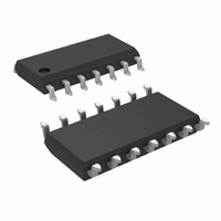
LM1815M/NOPB National Semiconductor, LM1815M/NOPB Datasheet - Page 2

LM1815M/NOPB
Manufacturer Part Number
LM1815M/NOPB
Description
IC ADAPTIVE SENSE AMP 14SOIC
Manufacturer
National Semiconductor
Type
Sensor Interfacer
Specifications of LM1815M/NOPB
Package / Case
14-SOIC (3.9mm Width), 14-SOL
Mounting Type
Surface Mount
Current - Supply
6mA
Output Type
Logic
Input Type
Logic
Lead Free Status / RoHS Status
Lead free / RoHS Compliant
Interface
-
Other names
*LM1815M::*LM1815M/NOPB::LM1815M
Available stocks
Company
Part Number
Manufacturer
Quantity
Price
Company:
Part Number:
LM1815M/NOPB
Manufacturer:
SONY
Quantity:
1 140
www.national.com
Operating Supply Voltage
Supply Current
Reference Pulse Width
Logic Input Bias Current
Signal Input Bias Current
Logic Threshold
V
V
Output Leakage Pin 12
Saturation Voltage P12
Input Zero Crossing Threshold
Minimum Input Arming
Threshold
Adaptive Input Arming
Threshold
OUT
OUT
Absolute Maximum Ratings
If Military/Aerospace specified devices are required,
please contact the National Semiconductor Sales Office/
Distributors for availability and specifications.
Electrical Characteristics
Note 1: “Absolute Maximum Ratings” are those values beyond which the safety of the device cannot be guaranteed. They are not meant to imply that the devices
should be operated at these limits. The table of “Electrical Characteristics” specifies conditions of device operation.
Note 2: For operation at elevated temperatures, the device must be derated based on a 150˚C maximum junction temperature and a thermal resistance of 80˚C/W
(DIP), 120˚C/W (SO-14) junction to ambient.
Note 3: Tested per Figure 1, V
Note 4: The Min/Typ Max limits are relative to the positive voltage peak seen at V
Supply Voltage
Power Dissipation (Note 2)
Operating Temperature Range
High
Low
Parameter
SIGNAL
is a Sine Wave; F
Pin 3 = -0.1V, Pin 9 = 2V, Pin 11 = 0.8V
f
V
V
(Pin 9 and Pin 11)
R
I
V
I
All Modes, V
Mode 1, Pin 5 = Open
Mode 2, Pin 5 = V
Mode 3, Pin 5 = Gnd
Mode 1, Pin 5 = Open
Mode 2, Pin 5 = V
Mode 3, Pin 5 = Gnd
IN
SINK
12
IN
IN
L
12
V
V
V
= 1Hz to 2kHz, R = 150kΩ, C = 0.001µF
= 1kΩ, (Pin 10)
= 2mA
SIGNAL
SIGNAL
SIGNAL
= 2V, (Pin 9 and Pin 11)
= 0V dc, (Pin 3)
= 11V
−40˚C ≤ T
= 0.1mA, (Pin 10)
≥ 230mV pk-pk (Note 3)
≥ 1.0V pk-pk (Note 3)
≥ 150mV pk-pk (Note 3)
(T
SIGNAL
SIGNAL
A
(Note 1)
A
= 25˚C, V
1250 mW
Conditions
≤ +125˚C
is 1000Hz.
CC
CC
= 1V pk-pk
12V
CC
= 10V, unless otherwise specified, see Figure 1)
2
IN
Pin 3.
Storage Temperature Range
Junction Temperature
Input Current
Lead Temperature
(Soldering, 10 sec.)
Min
200
2.5
0.8
7.5
-25
-25
70
30
40
-200
0.01
Typ
100
300
3.6
1.1
8.6
0.3
0.2
10
45
80
80
80
0
0
−65˚C ≤ T
Max
130
450
2.0
0.4
0.4
12
10
25
60
25
90
6
5
J
mV (Note 4)
mV (Note 4)
mV (Note 4)
mV (Note 4)
% (Note 4)
% (Note 4)
% (Note 4)
≤ +150˚C
±
+150˚C
Units
30 mA
260˚C
mA
µA
nA
µA
µs
V
V
V
V
V


