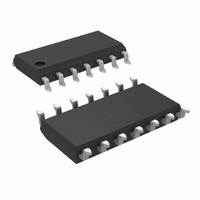
LM1815M/NOPB National Semiconductor, LM1815M/NOPB Datasheet - Page 10

LM1815M/NOPB
Manufacturer Part Number
LM1815M/NOPB
Description
IC ADAPTIVE SENSE AMP 14SOIC
Manufacturer
National Semiconductor
Type
Sensor Interfacer
Specifications of LM1815M/NOPB
Package / Case
14-SOIC (3.9mm Width), 14-SOL
Mounting Type
Surface Mount
Current - Supply
6mA
Output Type
Logic
Input Type
Logic
Lead Free Status / RoHS Status
Lead free / RoHS Compliant
Interface
-
Other names
*LM1815M::*LM1815M/NOPB::LM1815M
Available stocks
Company
Part Number
Manufacturer
Quantity
Price
Company:
Part Number:
LM1815M/NOPB
Manufacturer:
SONY
Quantity:
1 140
Application Hints
MODE 2, PIN 5 CONNECTED TO V+
The input arming threshold is fixed at 200mV minimum when
device pin 5 is connected to the positive supply. The chip has
no output for signals of less than
and triggers on the next negative-going zero crossing when
the arming threshold is has been exceeded.
MODE 3, PIN 5 GROUNDED
With pin 5 grounded, the input arming threshold is set to 0V,
chip, and the next negative-going zero crossing triggers it.
This is the very basic form of zero-crossing detection.
ONE SHOT TIMING
The one shot timing is set by a resistor and capacitor con-
nected to pin 14. The recommended maximum resistor value
is 150kohms. The capacitor value can be changed as
needed, as long as the capacitor type does not present any
signfigant leakage that would adversely affect the RC time
constant.
The output pulse width is:
±
25mV maximum. Positive-going zero crossings arm the
pulse width = 0.673 x R x C
(Continued)
±
200 mV (i.e. 400mVp-p)
(1)
9
For a given One Shot pulse width, the recommended maxi-
mum input signal frequency is:
In the application example shown in figure 1 (R=150kohms,
C=0.001µF) the recommended maximum input frequency
will typically be 5kHz. Operating with input frequencies
above the recommended Fin (max) value may result in
unreliable performance of the One Shot circuitry. For those
applications where the One Shot circuit is not required,
device pin 14 can be tied directly to Ground.
LOGIC INPUTS
In some systems it is necessary to externally generate
pulses, such as during stall conditions when the variable
reluctance sensor has no output. External pulse inputs at pin
9 are gated through to pin 10 when Input Select (pin 11) is
pulled high. Pin 12 is a direct output for the one shot and is
unaffected by the status of pin 11.
Input/output pins 9, 11, 10, and 12 are all CMOS logic
compatible. In addition, pins 9, 11, and 12 are TTL compat-
ible. Pin 10 is not guaranteed to drive a TTL load.
Pins 1, 4, 6 and 13 have no internal connections and can be
grounded.
Fin(max) = 1/(1.346 x R x C)
www.national.com
(2)


