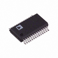
AD9822JRSZ Analog Devices Inc, AD9822JRSZ Datasheet - Page 14

AD9822JRSZ
Manufacturer Part Number
AD9822JRSZ
Description
IC CCD SIGNAL PROC 14BIT 28SSOP
Manufacturer
Analog Devices Inc
Type
CCD Signal Processor, 14-Bitr
Datasheet
1.AD9822JRSZRL.pdf
(20 pages)
Specifications of AD9822JRSZ
Input Type
Logic
Output Type
Logic
Interface
3-Wire Serial
Current - Supply
73mA
Mounting Type
Surface Mount
Package / Case
28-SSOP
Supply Voltage Range
3V To 5.25V, 4.75V To 5.25V
Power Dissipation Pd
450mW
Ic Mounting
SMD
Tv / Video Case Style
SSOP
No. Of Pins
28
Msl
MSL 3 - 168 Hours
Termination Type
SMD
Filter Terminals
SMD
Rohs Compliant
Yes
Digital Ic Case Style
SSOP
Lead Free Status / RoHS Status
Lead free / RoHS Compliant
Available stocks
Company
Part Number
Manufacturer
Quantity
Price
Company:
Part Number:
AD9822JRSZ
Manufacturer:
ADI
Quantity:
72
Part Number:
AD9822JRSZ
Manufacturer:
ADI/亚德诺
Quantity:
20 000
Part Number:
AD9822JRSZRL
Manufacturer:
ADI/亚德诺
Quantity:
20 000
AD9822
PGA Gain Registers
There are three PGA registers for individually programming the gain in the red, green, and blue channels. Bits D8, D7, and D6 in each
register must be set low, and Bits D5 through D0 control the gain range in 64 increments. See Figure 15 for the PGA gain vs. the PGA
register code. The coding for the PGA registers is straight binary, with an all 0s word corresponding to the minimum gain setting (1×)
and an all 1s word corresponding to the maximum gain setting (5.7×).
Table 9. PGA Gain Register Settings
D8
Set to 0
0
0
0
0
1
Offset Registers
There are three PGA registers for individually programming the offset in the red, green, and blue channels. Bits D8 through D0 control
the offset range from −350 mV to +350 mV in 512 increments. The coding for the offset registers is sign magnitude, with D8 as the sign
bit. Table 10 shows the offset range as a function of the Bits D8 through D0.
Table 10. Offset Register Settings
D8 (MSB)
0
0
0
1
1
1
1
Power-on default value.
Power-on default value.
D7
0
0
1
0
0
1
D7
Set to 0
0
0
0
0
D6
0
0
1
0
0
1
D6
Set to 0
0
0
0
0
D5
0
0
1
0
0
1
D5
MSB
0
0
1
1
D4
0
0
1
0
0
1
D4
0
0
1
1
Rev. B | Page 14 of 20
D3
0
0
•
•
•
1
0
0
•
•
•
1
D3
0
0
•
•
•
1
1
D2
0
0
1
0
0
1
D2
0
0
1
1
D1
0
0
1
1
D1
0
0
1
0
0
1
D0
LSB
0
1
0
1
1
D0 (LSB)
0
1
1
0
1
1
1
Gain (V/V)
1.0
1.013
•
•
•
5.4
5.7
Offset (mV)
0
+1.2
•
•
•
+350
0
−1.2
•
•
•
−350
Gain (dB)
0.0
0.12
•
•
•
14.6
15.1


