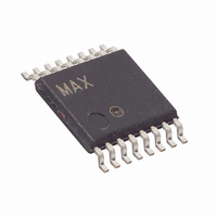
MXB7843EUE+ Maxim Integrated Products, MXB7843EUE+ Datasheet - Page 8

MXB7843EUE+
Manufacturer Part Number
MXB7843EUE+
Description
IC CNTRLR TOUCH RES 16TSSOP
Manufacturer
Maxim Integrated Products
Type
Resistiver
Datasheet
1.MXB7843EEE.pdf
(21 pages)
Specifications of MXB7843EUE+
Touch Panel Interface
4-Wire
Number Of Inputs/keys
1 TSC
Resolution (bits)
12 b
Data Interface
MICROWIRE™, QSPI™, Serial, SPI™
Data Rate/sampling Rate (sps, Bps)
125k
Voltage Reference
External
Voltage - Supply
2.38 V ~ 5.25 V
Current - Supply
650µA
Operating Temperature
-40°C ~ 85°C
Mounting Type
Surface Mount
Package / Case
16-TSSOP
Output Type
Digital
Interface
4-Wire Serial
Input Type
Analog
Lead Free Status / RoHS Status
Lead free / RoHS Compliant
The MXB7843 uses a successive-approximation conver-
sion technique to convert analog signals to a 12-bit digital
output. An SPI/QSPI/MICROWIRE™-compatible serial
interface provides an easy communication to a micro-
processor (µP). It features a 4-wire touch-screen interface
and two auxiliary ADC channels (Functional Diagram).
Figure 2 shows a block diagram of the analog input sec-
tion that includes the input multiplexer of the MXB7843,
the differential signal inputs of the ADC, and the differ-
ential reference inputs of the ADC. The input multiplexer
switches between X+, X-, Y+, Y-, IN3, and IN4.
In single-ended mode, conversions are performed using
REF as the reference. In differential mode, ratiometric
conversions are performed with REF+ connected to X+ or
Y+, and REF- connected to X- or Y-. Configure the refer-
ence and switching matrix according to Tables 1 and 2.
During the acquisition interval, the selected channel
charges the sampling capacitance. The acquisition
interval starts on the fifth falling clock edge and ends
on the eighth falling clock edge.
2.375V to 5.25V, 4-Wire Touch-Screen
Controller
Figure 1. Detailed Serial Interface Timing
MICROWIRE is a trademark of National Semiconductor Corp.
8
CS
DCLK
DIN
DOUT
BUSY
_______________________________________________________________________________________
t
t
BDV
t
DV
CSS
t
DS
Detailed Description
t
DH
t
CL
Analog Inputs
t
CH
The time required for the T/H to acquire an input signal
is a function of how quickly its input capacitance is
charged. If the input signal’s source impedance is high,
the acquisition time lengthens, and more time must be
allowed between conversions. The acquisition time
(t
the input signal to 12-bit accuracy. Calculate t
the following equation:
where R
the input signal.
Source impedances below 1kΩ do not significantly
affect the ADC’s performance. Accommodate higher
source impedances by either slowing down DCLK or
by placing a 1µF capacitor between the analog input
and GND.
The ADCs input tracking circuitry has a 25MHz small-
signal bandwidth, so it is possible to digitize high-
speed transient events. To avoid high-frequency sig-
nals being aliased into the frequency band of interest,
anti-alias filtering is recommended.
t
ACQ
CP
) is the maximum time the device takes to acquire
t
BD
IN
t
ACQ
= 2kΩ and R
Input Bandwidth and Anti-Aliasing
=
t
DO
8 4
.
×
S
(
R
is the source impedance of
S
+
R
IN
)
×
t
t
t
CSH
BTR
TR
25
pF
ACQ
with


