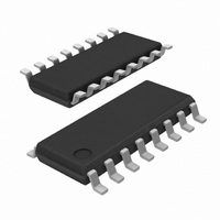
SI2493-C-FS Silicon Laboratories Inc, SI2493-C-FS Datasheet - Page 179

SI2493-C-FS
Manufacturer Part Number
SI2493-C-FS
Description
IC ISOMODEM SYSTEM-SIDE 16SOIC
Manufacturer
Silicon Laboratories Inc
Specifications of SI2493-C-FS
Mfg Application Notes
SI2493/57/34/15/04, Appl Note AN93
Data Format
V.21, V.22, V.23, V.29, V.32, V.34, V.90, V.92, Bell 103, Bell 212A
Baud Rates
56k
Interface
UART
Voltage - Supply
3 V ~ 3.6 V
Mounting Type
Surface Mount
Package / Case
16-SOIC (3.9mm Width)
Lead Free Status / RoHS Status
Lead free / RoHS Compliant
Available stocks
Company
Part Number
Manufacturer
Quantity
Price
Company:
Part Number:
SI2493-C-FSR
Manufacturer:
DY
Quantity:
8 623
Part Number:
SI2493-C-FSR
Manufacturer:
SIEMENS/西门子
Quantity:
20 000
- Current page: 179 of 230
- Download datasheet (7Mb)
Module Design and Application
Considerations
Modem modules are more susceptible to radiated fields
and ESD discharges than modems routed directly on
the motherboard because the module ground plane is
discontinuous and elevated above the motherboard
ground plane. This separation also creates the
possibility of loops that couple these interfering signals
to the modem. Additionally, system designers can
adversely impact the ESD and EMI immunity and
performance of a properly-designed module with a poor
motherboard layout.
Module Design
Particular attention should be paid to power supply
bypassing and reset line filtering when designing a
modem module. Trace routing is normally very short on
modules since they are generally designed to be as
small as possible. Care should be taken to use ground
and power planes in the low-voltage circuitry whenever
possible and to minimize the number of vias in the
ground and power traces. Ground and power should
each be connected to the motherboard through one pin
only to avoid the creation of loops. Bypassing and
filtering components should be placed as close to the
modem chip as possible with the shortest possible
traces to a solid ground. It is recommended that a pi
Motherboard
Connector
RESET
GND
VCC
1.0 μF
Figure 44. Modem Module V
.01 μF
Murata BLM 18A
G601 SN1
Rev. 0.9
filter be placed in series with the module V
filter (such as the one shown in Figure 29 on page 156)
on the reset line. This filter also provides a proper
power-on reset to the modem. Careful module design is
critical since the module designer frequently has little
control
environment in which the module will be used.
Motherboard Design
Motherboard design is critical to proper modem module
performance and immunity to EMI and ESD events.
First and foremost, good design and layout practices
must be followed. Use ground and power planes
whenever possible. Keep all traces short and direct.
Use ground fill on top and bottom layers. Use adequate
power supply bypassing, and use special precautions
with the power and reset lines to the modem module.
Bypass V
sure the modem module is connected to V
single pin. Likewise, be sure ground is connected to the
modem module through one pin connected to the
motherboard ground plane. The modem reset line is
sensitive and must be kept very short and routed well
away from any circuitry or components that could be
subjected to an ESD event. Finally, mount the modem
module as close to the motherboard as possible. Avoid
high-profile sockets that increase the separation
between the modem module and the motherboard.
CC
and RESET Filter
.01 μF
over
CC
right at the modem module connector. Be
the
motherboard
1.0 μF
To Modem Chip V
(Si2401 pins 5, 21)
10 kΩ
2.2 μF
design
(Si2401 pin 12)
To RESET
GND
CC
CC
AN93
pin with a
through a
and
CC
179
the
Related parts for SI2493-C-FS
Image
Part Number
Description
Manufacturer
Datasheet
Request
R
Part Number:
Description:
SOIC 16/C�/56 KBPS, V.92 ISOMODEM 16-PIN SYSTEM-SIDE - LEAD-FREE
Manufacturer:
Silicon Laboratories Inc
Part Number:
Description:
TSSOP 24/I�/56 KBPS, V.92 ISOMODEM SYSTEM-SIDE
Manufacturer:
Silicon Laboratories Inc
Part Number:
Description:
IC ISOMODEM SYSTEM-SIDE 24TSSOP
Manufacturer:
Silicon Laboratories Inc
Datasheet:
Part Number:
Description:
56 KBPS, V.92 ISOMODEM SYSTEM-SIDE - LEAD-FREE TSSOP 0 TO 7
Manufacturer:
Silicon Laboratories Inc
Datasheet:
Part Number:
Description:
Telecom ICs CONTACT SILICON LABS FOR AVAILABILITY
Manufacturer:
Silicon Laboratories Inc
Part Number:
Description:
IC ISOMODEM SYSTEM-SIDE 16SOIC
Manufacturer:
Silicon Laboratories Inc
Datasheet:
Part Number:
Description:
IC ISOMODEM SYSTEM-SIDE 24TSSOP
Manufacturer:
Silicon Laboratories Inc
Datasheet:

Part Number:
Description:
IC ISOMODEM W/ERROR CORR 16SOIC
Manufacturer:
Silicon Laboratories Inc
Datasheet:
Part Number:
Description:
IC ISOMODEM W/ERROR CORR 24TSSOP
Manufacturer:
Silicon Laboratories Inc
Datasheet:

Part Number:
Description:
IC ISOMODEM W/DAA 16SOIC
Manufacturer:
Silicon Laboratories Inc
Datasheet:
Part Number:
Description:
IC ISOMODEM SYSTEM-SIDE 24TSSOP
Manufacturer:
Silicon Laboratories Inc
Datasheet:
Part Number:
Description:
IC ISOMODEM W/ERROR CORR 24TSSOP
Manufacturer:
Silicon Laboratories Inc
Datasheet:
Part Number:
Description:
IC ISOMODEM W/DAA 24TSSOP
Manufacturer:
Silicon Laboratories Inc
Datasheet:


