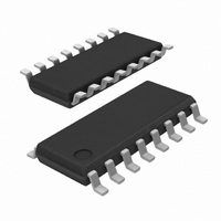
SI3010-F-FS Silicon Laboratories Inc, SI3010-F-FS Datasheet - Page 10

SI3010-F-FS
Manufacturer Part Number
SI3010-F-FS
Description
IC SI2401 ISOMOD LINESIDE 16SOIC
Manufacturer
Silicon Laboratories Inc
Type
Chipsetr
Datasheet
1.SI3056-D-FS.pdf
(94 pages)
Specifications of SI3010-F-FS
Package / Case
16-SOIC (3.9mm Width)
Data Format
V.92
Interface
Serial
Voltage - Supply
3 V ~ 3.6 V
Mounting Type
Surface Mount
Product
Modem Module
Supply Voltage (min)
3 V
Supply Current
10 mA
Maximum Operating Temperature
+ 70 C
Minimum Operating Temperature
0 C
Mounting Style
SMD/SMT
Lead Free Status / RoHS Status
Lead free / RoHS Compliant
Baud Rates
-
Lead Free Status / RoHS Status
Lead free / RoHS Compliant, Lead free / RoHS Compliant
Other names
336-1286-5
Available stocks
Company
Part Number
Manufacturer
Quantity
Price
Company:
Part Number:
SI3010-F-FS
Manufacturer:
YCL
Quantity:
105
Part Number:
SI3010-F-FS
Manufacturer:
SILICONI/矽睿科技
Quantity:
20 000
Company:
Part Number:
SI3010-F-FSR
Manufacturer:
SILICON
Quantity:
2 650
Company:
Part Number:
SI3010-F-FSR
Manufacturer:
Silicon
Quantity:
702
Part Number:
SI3010-F-FSR
Manufacturer:
SILICON LABS/芯科
Quantity:
20 000
Si3018/19/10
Table 5. Absolute Maximum Ratings
10
Table 6. Switching Characteristics—General Inputs
(V
Parameter
DC Supply Voltage
Input Current, Si3056 Digital Input Pins
Digital Input Voltage
Operating Temperature Range
Storage Temperature Range
Note: Permanent device damage can occur if the above absolute maximum ratings are exceeded. Restrict functional
Parameter
Cycle Time, MCLK
MCLK Duty Cycle
MCLK Jitter Tolerance
Rise Time, MCLK
Fall Time, MCLK
MCLK Before RESET ↑
RESET Pulse Width
M0, M Before RESET↑
Notes:
D
RESET
M 0, M1
=
1. All timing (except Rise and Fall time) is referenced to the 50% level of the waveform. Input test levels are
2. The minimum RESET pulse width is the greater of 250 ns or 10 MCLK cycle times.
3. M0 and M are typically connected to V
M CLK
3.0 to 3.6 V, T
operation to the conditions as specified in the operational sections of this data sheet. Exposure to absolute maximum
rating conditions for extended periods might affect device reliability.
V
IH
=
1
V
D
– 0.4 V, V
A
=
2
0 to 70 °C, C
3
IL
=
0.4 V. Rise and fall times are referenced to the 20% and 80% levels of the waveform.
Figure 2. General Inputs Timing Diagram
L
=
20 pF)
D
or GND and should not be changed during normal operation.
Symbol
T
V
Rev. 1.05
Symbol
V
I
T
STG
IND
IN
D
A
t
t
t
t
t
rl
jitter
t
mxr
mc
dty
t
mr
t
t
rl
r
f
t
t
m xr
r
16.67
Min
250
40
10
20
—
—
—
t
–0.3 to (V
m r
–0.5 to 3.6
–40 to 100
–65 to 150
t
m c
Value
±10
D
Typ
50
+ 0.3)
—
—
—
—
—
—
—
1000
Max
60
±2
—
—
—
5
5
t
f
Unit
mA
°C
°C
V
V
cycles
Unit
ns
ns
ns
ns
ns
ns
%
V
V
IH
IL


