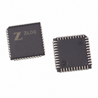
Z0220112VEGR4078 Zilog, Z0220112VEGR4078 Datasheet - Page 29

Z0220112VEGR4078
Manufacturer Part Number
Z0220112VEGR4078
Description
IC MODEM 2400BPS DSP AFE 44-PLCC
Manufacturer
Zilog
Specifications of Z0220112VEGR4078
Data Format
V.21, V.22, V.23, Bell 103, Bell 212A
Baud Rates
2.4k
Interface
Parallel
Voltage - Supply
4.5 V ~ 5.5 V
Mounting Type
Surface Mount
Package / Case
44-LCC (J-Lead)
Lead Free Status / RoHS Status
Lead free / RoHS Compliant
Available stocks
Company
Part Number
Manufacturer
Quantity
Price
Table 16. REG4: RAM Control Register
PS000904-0107
SYMBOL
RAMAH
RAMRQ
RAMRW
RTSP
TPDM
Note: All the bits in this register (REG 4) default to logic 0 at power-up or after reset sequences are completed.
Bit
Microprocessor Interface Register and Bit Definitions:
TXIE
7
POSITION
REG 4, bit 0
REG 4, bit 1
REG 4, bit 2
REG 4, bit 3
REG 4, bit 4
Reg0, Reg1 RAMDL, RAMDH—DATA PUMP RAM DATA REGISTERS—
RAMDL is the least significant byte, and RAMDH is the most significant byte.
After a data pump RAM read operation has completed, these registers contain the
requested data. When a data pump RAM write operation is started, these regis-
ters contain the data written to data pump RAM.
Reg2 RAMAL—DATA PUMP RAM DATA ADDRESS—
read or write operation is started, this byte contains the lower 8 bits of the RAM
address. Register 4 (RAMAH) is the high bit of the RAM address.
Reg3 DATAP—DATA PUMP PARALLEL DATA—
ferred to or from the remote modem during the parallel modem (see register Reg-
ister 4, bit 4). At any reset, when Config register bits 0–6 (MODE) is
the data pump places its firmware version number in register DATAP.
RXIE
6
RAMIE
NAME AND DESCRIPTION
RAM Address High Bit. The most significant bit of the data pump RAM
address. This bit is set to 1 when accessing a data pump RAM address
that is greater than 255, or set to 0 for any value below 255.
Data Pump RAM Access Request Bit. Set this bit to 1 to request a read or
write of the data pump RAM. The data pump sets this bit to 0 when the
request has been fulfilled.
Data Pump RAM Read/Write Bit. Set this bit to 0 to request a read of the
data pump RAM or a 1 to request a write of data pump RAM.
Register Request to Send Bit. A logical OR operation is executed using the
value of the hardware RTS signal received by the data pump on the RTS
pin. The host sets RTS or RTSP to 1 to inform the data pump the host is
transmitting data. To control the data pump using the RTS signal, set
RTSP to 0. To control the data pump using RTSP, hold RTS High.
Select Parallel Data Mode. Setting this bit selects the parallel data mode.
Resetting it selects the serial data mode.
5
TPDM
4
RTSP
3
V.22BIS Data Pump with Integrated AFE
RAMRW RAMRQ
2
This register contains data trans-
When a data pump RAM
1
RAMAH
0
0
(STANDBY),
In this case,
25


