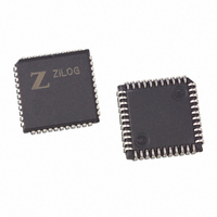
Z0220112VSGR3470 Zilog, Z0220112VSGR3470 Datasheet - Page 14

Z0220112VSGR3470
Manufacturer Part Number
Z0220112VSGR3470
Description
IC MODEM 2400BPS DSP AFE 44-PLCC
Manufacturer
Zilog
Specifications of Z0220112VSGR3470
Data Format
V.21, V.22, V.23, Bell 103, Bell 212A
Baud Rates
2.4k
Interface
Parallel
Voltage - Supply
4.5 V ~ 5.5 V
Mounting Type
Surface Mount
Package / Case
44-LCC (J-Lead)
Lead Free Status / RoHS Status
Lead free / RoHS Compliant
Available stocks
Company
Part Number
Manufacturer
Quantity
Price
Z02201
V.22BIS Data Pump with Integrated AFE
10
This signal is used for
EYESTB Serial Eye Pattern Strobe (Output, Active High)—
loading an external D/A converter.
The TXO+,
TXO+ Transmit Differential Analog Output Positive (Analog Output)—
TXO– is capable of driving a 600-ohm resistive load over a leased line or public
switched telephone network via a Data Access Arrangement (DAA). The TXO–
and TXO+ can be configured either as a differential or single-ended output driver.
The TXO–,
TXO– Transmit Differential Analog Output Negative (Analog Output)—
TXO+ is capable of driving a 600-ohm resistive load over a leased line or public
switched telephone network via a Data Access Arrangement (DAA).
RXI– Receive Differential Analog Input Negative (Analog Input)—
RXI+ Receive Differential Analog Input Positive (Analog Input)—
This pin is a test pin and must be tied to
TEST1 Test Pin 1 (Input, Active High)—
digital ground.
This pin is a
TEST2/RCLK Test Pin 2, Receive Data Clock (Output, Active High)—
test pin and must be tied to digital ground through a pull-down resistor. The resis-
tor should be Low enough to ensure this pin floats below 0.8V when the part is in
the RESET state. After RESET, this pin becomes the Receive Data Clock Output.
The resistor should be high enough such that the output can be driven to logic
.
1
This pin is a synchronous data clock used to transfer serial data between the data
pump and the host. The clock frequencies are 2400, 1200, and 300 Hz corre-
sponding to the supported data bit rates.
An internally generated reference
Vref Reference Voltage (Output, Active High—
voltage.
Crystal oscillator connection. This pin must
XTAL Crystal (Output, Active High)—
be left open if an external clock is used instead of a crystal. The data pump chip
can be connected to an external crystal circuit consisting of 24.576-MHz (parallel
resonant) crystal, a resistor, and two capacitors.
Crystal oscillator connection.
EXTAL External Clock/ Crystal (Input, Active High)—
An external clock can be input to the Z02280 on this pin when a crystal is not
used. The oscillator input is not a TTL level (see DC characteristics in Table 4).
Connect an 82pF
CF1 and CF2 Integration Capacitor Pins 1 and 2 (Analog Input)—
capacitor between CF2 and CF1 to complete the internal feedback integration fil-
ter for improved Analog-to-Digital (A/D) conversion performance.
GND Digital ground–0 Volts—
V
Digital Power–5 Volts—
DD
AV
Analog Power–5 Volts—
DD
AGND Analog Ground–0 Volts—
PS000904-0107


