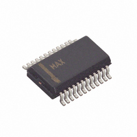
MAX7325AEG+T Maxim Integrated Products, MAX7325AEG+T Datasheet - Page 8

MAX7325AEG+T
Manufacturer Part Number
MAX7325AEG+T
Description
IC I/O EXPANDER I2C 8B 24QSOP
Manufacturer
Maxim Integrated Products
Datasheet
1.MAX7325AEG.pdf
(19 pages)
Specifications of MAX7325AEG+T
Interface
I²C
Number Of I /o
8
Interrupt Output
Yes
Frequency - Clock
400kHz
Voltage - Supply
1.71 V ~ 5.5 V
Operating Temperature
-40°C ~ 125°C
Mounting Type
Surface Mount
Package / Case
24-QSOP
Includes
POR
Lead Free Status / RoHS Status
Lead free / RoHS Compliant
I
and 8 Open-Drain I/Os
connected to V+ or GND. This is important because the
address selection is used to determine the power-up
logic state and whether pullups are enabled. At power-
up, the I
impedance at the inputs of every device (master or
slave) connected to the bus, including the MAX7325.
This is guaranteed as part of the I
Therefore, when address inputs AD0 and AD2 are con-
nected to SDA or SCL during power-up, they appear to
be connected to V+.
The power-up logic uses AD0 to select the power-up
state and whether pullups are enabled for ports P0–P3,
and AD2 for ports P4–P7. The rule is that a logic-high,
SDA, or SCL connection selects the pullups and sets
the default logic state to high. A logic-low deselects the
pullups and sets the default logic state to low (Table 2).
The port configuration is correct on power-up for a
standard I
pulled up to V+ by the external I
Table 2. MAX7325 Address Map for Ports P0–P7
8
CONNECTION
GND
GND
GND
GND
AD2
SDA
SDA
SDA
SDA
2
SCL
SCL
SCL
SCL
V+
V+
V+
V+
_______________________________________________________________________________________
C Port Expander with 8 Push-Pull
PIN
2
GND
GND
GND
GND
AD0
SDA
SDA
SDA
SDA
SCL
SCL
SCL
SCL
C SDA and SCL bus interface lines are high
V+
V+
V+
V+
2
C configuration, where SDA or SCL are
A6 A5 A4 A3 A2 A1 A0
1
1
1
1
1
1
1
1
1
1
1
1
1
1
1
1
1
1
1
1
1
1
1
1
1
1
1
1
1
1
1
1
DEVICE ADDRESS
0
0
0
0
0
0
0
0
0
0
0
0
0
0
0
0
0
0
0
0
0
0
0
0
1
1
1
1
1
1
1
1
2
C pullup resistors.
0
0
0
0
1
1
1
1
0
0
0
0
1
1
1
1
2
0
0
1
1
0
0
1
1
0
0
1
1
0
0
1
1
C specification.
0
1
0
1
0
1
0
1
0
1
0
1
0
1
0
1
P7
1
1
1
1
1
1
1
1
0
0
0
0
1
1
1
1
PORT POWER-UP DEFAULT
P6
1
1
1
1
1
1
1
1
0
0
0
0
1
1
1
1
P5
1
1
1
1
1
1
1
1
0
0
0
0
1
1
1
1
P4
There are circumstances where the assumption that
SDA = SCL = V+ on power-up is not true—for example,
in applications in which there is legitimate bus activity
during power-up. If SDA and SCL are terminated with
pullup resistors to a different supply voltage than the
MAX7325’s supply voltage, and if that pullup supply
rises later than the MAX7325’s supply, then SDA or
SCL may appear at power-up to be connected to GND.
In such applications, use the four address combina-
tions that are selected by connecting address inputs
AD0 and AD2 to V+ or GND (shown in bold in Tables 2
and 3). These selections are guaranteed to be correct
at power-up, independent of SDA and SCL behavior. If
one of the other 12 address combinations is used, an
unexpected combination of pullups might be asserted
until the first I
sarily the MAX7325) is put on the bus, and an unex-
pected combination of ports can initialize as logic-low
outputs instead of inputs or logic-high outputs.
1
1
1
1
1
1
1
1
0
0
0
0
1
1
1
1
P3
0
1
1
1
0
1
1
1
0
1
1
1
0
1
1
1
P2
0
1
1
1
0
1
1
1
0
1
1
1
0
1
1
1
2
P1
0
1
1
1
0
1
1
1
0
1
1
1
0
1
1
1
C transmission (to any device, not neces-
P0
0
1
1
1
0
1
1
1
0
1
1
1
0
1
1
1
—
—
—
—
P7 P6 P5 P4 P3 P2 P1 P0
Y
Y
Y
Y
Y
Y
Y
Y
Y
Y
Y
Y
40kΩ INPUT PULLUPS ENABLED
—
—
—
—
Y
Y
Y
Y
Y
Y
Y
Y
Y
Y
Y
Y
—
—
—
—
Y
Y
Y
Y
Y
Y
Y
Y
Y
Y
Y
Y
—
—
—
—
Y
Y
Y
Y
Y
Y
Y
Y
Y
Y
Y
Y
—
—
—
—
Y
Y
Y
Y
Y
Y
Y
Y
Y
Y
Y
Y
—
—
—
—
Y
Y
Y
Y
Y
Y
Y
Y
Y
Y
Y
Y
—
—
—
—
Y
Y
Y
Y
Y
Y
Y
Y
Y
Y
Y
Y
—
—
—
—
Y
Y
Y
Y
Y
Y
Y
Y
Y
Y
Y
Y


