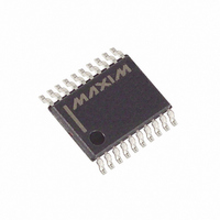
DS4550E+T&R Maxim Integrated Products, DS4550E+T&R Datasheet

DS4550E+T&R
Specifications of DS4550E+T&R
Related parts for DS4550E+T&R
DS4550E+T&R Summary of contents
Page 1
... I/O_8 18 I/O_7 17 I/O_6 16 I/O_5 TDO INTERFACE 13 TDI 12 SCL JTAG INTERFACE 11 SDA ______________________________________________ Maxim Integrated Products Features Ordering Information TEMP RANGE PIN-PACKAGE -40°C to +85°C 20 TSSOP Typical Operating Circuit V CC DS4550 V CC I/O_0 A0 I/O_1 A1 I/O_2 4.7k A2 I/O_3 GND I/O_4 I/O_5 SCL ...
Page 2
I C and JTAG Nonvolatile 9-Bit I/O Expander Plus Memory ABSOLUTE MAXIMUM RATINGS Voltage SDA, and SCL Pins CC Relative to Ground.............................................-0.5V to +6.0V Voltage on A0, A1, A2, TCK, TMS, TDI, and I/O_n [n = ...
Page 3
I AC ELECTRICAL CHARACTERISTICS-– +2.7V to +5.5V -40°C to +85°C, unless otherwise noted. Timing referenced PARAMETER SYMBOL SCL Clock Frequency Bus Free Time Between Stop and Start Conditions Hold Time (Repeated) Start ...
Page 4
I C and JTAG Nonvolatile 9-Bit I/O Expander Plus Memory NONVOLATILE MEMORY CHARACTERISTICS (V = +2.7V to +5.5V, unless otherwise noted.) CC PARAMETER SYMBOL EEPROM Writes Note 1: All voltages referenced to ground. Note specified with ...
Page 5
+5.0V +25°C; TDI, TDO, TMS pins are no connects, unless otherwise noted SUPPLY CURRENT vs. SUPPLY VOLTAGE 2 I/O0-I/O7 CONTROL BITS = 0 I/O0-I/O7 PULLUPS DISABLED V = SDA = SCL = TCK ...
Page 6
I C and JTAG Nonvolatile 9-Bit I/O Expander Plus Memory PIN NAME 1 I/O_0 Input/Output 0. Bidirectional I/O pin. 2 I/O_1 Input/Output 1. Bidirectional I/O pin. 3 I/O_2 Input/Output 2. Bidirectional I/O pin. 4 I/O_3 Input/Output 3. Bidirectional I/O ...
Page 7
SDA BSC SCL BSC BSC INTERFACE BSC A1 A2 BSC V CC EEPROM 64 BYTES USER MEMORY R R JPU JPU TMS JTAG TDI CONTROL TDO PORT TCK GND Detailed Description ...
Page 8
I C and JTAG Nonvolatile 9-Bit I/O Expander Plus Memory Memory Map and Memory Types The DS4550 memory map is shown in different types of memory are present in the DS4550: EEPROM, SRAM-shadowed EEPROM, and SRAM. Memory locations specified ...
Page 9
I Slave Address and Address Pins 2 The DS4550’ slave address is determined by the state of the A0, A1, and A2 address pins as shown in Figure 2. Address pins connected to GND result in a ‘0’ ...
Page 10
I C and JTAG Nonvolatile 9-Bit I/O Expander Plus Memory Test Access Port (TAP) Controller State Machine The TAP controller is a finite state machine that responds to the logic level at TMS on the rising edge of TCK ...
Page 11
I Update-DR. A falling edge on TCK while in the Update-DR state latches the data from the shift regis- ter path of the test data registers into a set of output latches. This prevents changes at the parallel output because ...
Page 12
I C and JTAG Nonvolatile 9-Bit I/O Expander Plus Memory CLAMP. All digital outputs of the device output data from the Boundary Scan parallel output while connect- ing the Bypass test data register between TDI and TDO. The outputs ...
Page 13
I Table 3. Boundary Scan Control Bits [33 Bits] CELL NAME NUMBER 32 A2 input 31 A1 input 30 A0 input 29 SCL input 28 SDA input 27 SDA output 26 IO8 pubout 25 IO8 pdbout 24 IO8 input 23 ...
Page 14
I C and JTAG Nonvolatile 9-Bit I/O Expander Plus Memory Table 5. EEPROM Write Cycle STEP TAP STATE Select-IR-Scan Capture-IR Select Address Shift- TCK) Register Exit1-IR Update-IR Select-DR-Scan Capture-DR Load EEPROM Shift- TCK) Address Exit1-DR ...
Page 15
I Bit Read: At the end a write operation, the master must release the SDA bus line for the proper amount of setup time (see Figure 5) before the next rising edge of SCL during a bit read. The device ...
Page 16
I C and JTAG Nonvolatile 9-Bit I/O Expander Plus Memory The DS4550’s slave address of the DS4550 is deter- mined by the state of the A0, A1, and A2 address pins as shown in Figure 2. Address pins connected ...
Page 17
I See Figure 6 for a read example using the repeated start condition to specify the starting memory location. Reading Multiple Bytes from a Slave: The read oper- ation can be used to read multiple bytes with a single transfer. ...
Page 18
... Maxim cannot assume responsibility for use of any circuitry other than circuitry entirely embodied in a Maxim product. No circuit patent licenses are implied. Maxim reserves the right to change the circuitry and specifications without notice at any time. 18 ____________________Maxim Integrated Products, 120 San Gabriel Drive, Sunnyvale, CA 94086 408-737-7600 © 2004 Maxim Integrated Products is a registered trademark of Dallas Semiconductor Corporation. ...


