CMQ82C55AZ96 Intersil, CMQ82C55AZ96 Datasheet
CMQ82C55AZ96
Specifications of CMQ82C55AZ96
Available stocks


Related parts for CMQ82C55AZ96

CMQ82C55AZ96 Summary of contents
Page 1
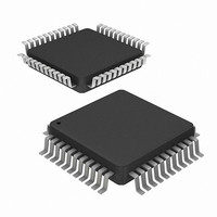
... Ld MQFP Q44.10x10 CAUTION: These devices are sensitive to electrostatic discharge; follow proper IC Handling Procedures. 1-888-INTERSIL or 1-888-468-3774 All other trademarks mentioned are the property of their respective owners. FN6140.2 | Intersil (and design registered trademark of Intersil Americas Inc. Copyright Intersil Americas Inc. 2005-2006. All Rights Reserved ...
Page 2
Pinouts MS82C55A (PLCC) TOP VIEW GND PC7 PC6 13 PC5 14 PC4 15 16 PC0 PC1 ...
Page 3
Pin Description SYMBOL TYPE The +5V power supply pin. A 0.1µF capacitor between GND GROUND D0-D7 I/O DATA BUS: The Data Bus lines are bidirectional three-state pins connected to the system data bus. RESET ...
Page 4
Functional Description Data Bus Buffer This three-state bidirectional 8-bit buffer is used to interface the 82C55A to the system data bus. Data is transmitted or received by the buffer upon execution of input or output instructions by the CPU. Control ...
Page 5
Operational Description Mode Selection There are three basic modes of operation than can be selected by the system software: Mode 0 - Basic Input/Output Mode 1 - Strobed Input/Output Mode 2 - Bidirectional Bus When the reset input goes “high”, ...
Page 6
CONTROL WORD BIT SET/RESET SET 0 = RESET DON’T CARE BIT SELECT BIT SET/RESET FLAG 0 = ACTIVE FIGURE 5. BIT SET/RESET FORMAT Interrupt Control Functions When ...
Page 7
Mode 0 (Basic Output) WR D7-D0 CS, A1, A0 OUTPUT Mode 0 Configurations CONTROL WORD # 82C55A CONTROL ...
Page 8
Mode 0 Configurations (Continued) CONTROL WORD # 82C55A CONTROL WORD # ...
Page 9
Mode 0 Configurations (Continued) CONTROL WORD # 82C55A Operating Modes Mode 1 - (Strobed Input/Output). This functional configuration ...
Page 10
MODE 1 (PORT A) CONTROL WORD INTE 1/0 PC6, PC7 1 = INPUT 0 = OUTPUT RD STB IBF INTR RD INPUT FROM PERIPHERAL ACK - (Acknowledge Input). ...
Page 11
WR OBF INTR ACK OUTPUT RD CONTROL WORD 1 PC6, PC7 1 = INPUT 0 = OUTPUT WR PORT A - (STROBED INPUT) PORT B - ...
Page 12
CONTROL WORD 1/0 1/0 1/0 FIGURE 11. MODE CONTROL WORD DATA FROM CPU TO 82C55A WR OBF INTR ACK STB IBF PERIPHERAL BUS RD NOTE: Any sequence where WR occurs ...
Page 13
MODE 2 AND MODE 0 (INPUT) CONTROL WORD 1/0 PC2-PC0 1 = INPUT 0 = OUTPUT RD WR MODE 2 AND MODE 1 (OUTPUT) CONTROL WORD D7 D6 ...
Page 14
MODE 0 IN PA0 In PA1 In PA2 In PA3 In PA4 In PA5 In PA6 In PA7 In PB0 In PB1 In PB2 In PB3 In PB4 In PB5 In PB6 In PB7 In PC0 In PC1 In PC2 ...
Page 15
Reading Port C Status (Figures 15 and 16) In Mode 0, Port C transfers data to or from the peripheral device. When the 82C55A is programmed to function in Modes Port C generates or accepts “hand shaking” ...
Page 16
MS82C55A, MQ82C55A, MP82C55A INTERRUPT REQUEST PC3 PA0 R0 PA1 R1 PA2 R2 PA3 R3 DECODED PA4 R4 KEYBOARD PA5 R5 MODE 1 PA6 SHIFT (INPUT) PA7 CONTROL PC4 STROBE PC5 ACK 82C55A PB0 B0 PB1 B1 PB2 B2 BURROUGHS PB3 ...
Page 17
INTERRUPT REQUEST PC3 PA0 D0 PA1 D1 PA2 D2 PA3 D3 CONTROLLER PA4 D4 PA5 D5 MODE 2 PA6 D6 PA7 D7 PC4 DATA STB PC5 ACK (IN) PC7 DATA READY PC6 ACK (OUT) 82C55A PC2 TRACK “0” SENSOR PC1 ...
Page 18
Absolute Maximum Ratings T = 25°C A Supply Voltage . . . . . . . . . . . . . . . . . . . . . . . . . . . . . . . ...
Page 19
AC Electrical Specifications V SYMBOL READ TIMING (1) tAR Address Stable Before RD (2) tRA Address Stable After RD (3) tRR RD Pulse Width (4) tRD Data Valid From RD (5) tDF Data Float After RD (6) tRV Time Between ...
Page 20
Timing Waveforms RD INPUT CS, A1, A0 D7-D0 WR D7-D0 CS, A1, A0 OUTPUT STB IBF INTR RD INPUT FROM PERIPHERAL 20 MS82C55A, MQ82C55A, MP82C55A tRR (3) tIR (13) tAR (1) tRD (4) FIGURE 25. MODE 0 (BASIC INPUT) tWW ...
Page 21
Timing Waveforms (Continued) WR OBF INTR ACK OUTPUT DATA FROM CPU TO 82C55A WR OBF INTR ACK STB IBF PERIPHERAL BUS RD NOTE: Any sequence where WR occurs before ACK and STB occurs before RD is permissible. (INTR = IBF ...
Page 22
Timing Waveforms (Continued) A0-A1, CS tAW (7) DATA BUS tDW (10) WR tWW (9) FIGURE 30. WRITE TIMING AC Test Circuit V1 R1 OUTPUT FROM DEVICE UNDER TEST R2 NOTE: Includes STRAY and JIG Capacitance 22 MS82C55A, MQ82C55A, MP82C55A A0-A1, ...
Page 23
Die Characteristics METALLIZATION: Type: Silicon - Aluminum ± Å Å Thickness: 11k 1k Metallization Mask Layout CS GND A1 A0 PC7 PC6 PC5 PC4 PC0 PC1 23 MS82C55A, MQ82C55A, MP82C55A GLASSIVATION: Type: SiO Thickness: 8k 82C55A RD PA0 PA1 PA2 ...
Page 24
Dual-In-Line Plastic Packages (PDIP INDEX N/2 AREA -B- -A- D BASE PLANE -C- SEATING PLANE 0.010 (0.25 NOTES: 1. Controlling Dimensions: INCH. In case of conflict between ...
Page 25
Plastic Leaded Chip Carrier Packages (PLCC) 0.042 (1.07) 0.042 (1.07) 0.048 (1.22) 0.056 (1.42) PIN (1) IDENTIFIER 0.050 (1.27 0.020 (0.51) MAX 3 PLCS 0.026 (0.66) 0.032 (0.81) 0.045 (1.14) MIN VIEW “A” ...
Page 26
... Accordingly, the reader is cautioned to verify that data sheets are current before placing orders. Information furnished by Intersil is believed to be accurate and reliable. However, no responsibility is assumed by Intersil or its subsidiaries for its use; nor for any infringements of patents or other rights of third parties which may result from its use ...