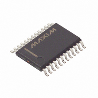
MAX7318AUG+ Maxim Integrated Products, MAX7318AUG+ Datasheet - Page 3

MAX7318AUG+
Manufacturer Part Number
MAX7318AUG+
Description
IC I/O EXPANDER I2C 16B 24TSSOP
Manufacturer
Maxim Integrated Products
Datasheet
1.MAX7318AUG.pdf
(19 pages)
Specifications of MAX7318AUG+
Interface
I²C, SMBus
Number Of I /o
16
Interrupt Output
Yes
Frequency - Clock
400kHz
Voltage - Supply
2 V ~ 5.5 V
Operating Temperature
-40°C ~ 125°C
Mounting Type
Surface Mount
Package / Case
24-TSSOP
Includes
POR
Lead Free Status / RoHS Status
Lead free / RoHS Compliant
DC ELECTRICAL CHARACTERISTICS (continued)
(V+ = 2V to 5.5V, T
AC ELECTRICAL CHARACTERISTICS
(V+ = 2V to 5.5V, T
Note 1: All parameters are 100% production tested at T
Note 2: A master device must internally provide a hold time of at least 300ns for the SDA signal (referred to the V
Note 3: C
Note 4: The maximum t
Note 5: Input filters on the SDA and SCL inputs suppress noise spikes less than 50ns.
Leakage Current
Input Capacitance
INT
Low-Level Output Current
SCL Clock Frequency
Bus Free Time Between STOP
and START Conditions
Hold Time (Repeated) START
Condition
Repeated START Condition
Setup Time
STOP Condition Setup Time
Data Hold Time
Data Setup Time
SCL Low Period
SCL High Period
SDA Fall Time
Pulse Width of Spike Suppressed
PORT TIMING
Output Data Valid
Input Data Setup Time
Input Data Hold Time
INTERRUPT TIMING
Interrupt Valid
Interrupt Reset
signal) to bridge the undefined region SCL’s falling edge.
specified at 250ns. This allows series protection resistors to be connected between the SDA and SCL pins and the SDA/SCL
bus lines without exceeding the maximum specified t
B
PARAMETER
PARAMETER
= total capacitance of one bus line in pF.
2-Wire-Interfaced, 16-Bit, I/O Port Expander
with Interrupt and Hot-Insertion Protection
A
A
= -40°C to +125°C, unless otherwise noted. Typical values are at V+ = 3.3V, T
= -40°C to +125°C, unless otherwise noted.) (Note 1)
_______________________________________________________________________________________
F
for the SDA and SCL bus lines is specified at 300ns. The maximum fall time for the SDA output stage t
SYM B O L
SYM B O L
t
t
t
t
t
HD,DAT
HD,STA
SU,STA
SU,STO
SU,DAT
t
t
t
f
HIGH
LOW
I
BUF
SCL
t
t
t
OL
t
t
SP
PV
IR
IV
F
V
Figure 2
Figure 2
Figure 2
Figure 2
Figure 2 (Note 2)
Figure 2
Figure 2
Figure 2
Figure 2 (Notes 3, 4)
(Note 5)
Figure 7
Figure 9
Figure 9
OL
= 0.4V
A
= +25°C. Specifications over temperature are guaranteed by design.
F
.
CONDITIONS
CONDITIONS
V+ < 3.3V
V+ ≥ 3.3V
MIN
MIN
100
1.3
0.6
0.6
0.6
1.3
0.7
27
A
-1
6
0
= +25°C.) (Note 1)
TYP
TYP
50
4
MAX
MAX
30.5
400
500
250
0.9
+1
3
2
IL
of the SCL
UNITS
UNITS
kHz
mA
µA
pF
µs
µs
µs
µs
µs
ns
µs
µs
ns
ns
µs
µs
µs
µs
µs
F
is
3


