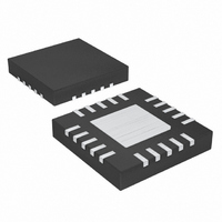
MAX7313ATG+ Maxim Integrated Products, MAX7313ATG+ Datasheet - Page 16

MAX7313ATG+
Manufacturer Part Number
MAX7313ATG+
Description
IC I/O EXPANDER I2C 16B 24TQFN
Manufacturer
Maxim Integrated Products
Datasheet
1.MAX7313ATG.pdf
(27 pages)
Specifications of MAX7313ATG+
Interface
I²C
Number Of I /o
16
Interrupt Output
Yes
Frequency - Clock
400kHz
Voltage - Supply
2 V ~ 3.6 V
Operating Temperature
-40°C ~ 125°C
Mounting Type
Surface Mount
Package / Case
24-TQFN Exposed Pad
Lead Free Status / RoHS Status
Lead free / RoHS Compliant
Set the interrupt enable I bit in the configuration register
to configure INT/O16 as the INT output (Table 4). Clear
interrupt enable to configure INT/O16 as the O16. O16
logic state is set by the 2 bits O1 and O0 in the configu-
ration register. O16 follows the rules for blinking select-
ed by the blink enable flag E in the configuration
register. If blinking is disabled, then interrupt output
control O0 alone sets the logic state of the INT/O16 pin.
If blinking is enabled, then both interrupt output con-
trols O0 and O1 set the logic state of the INT/O16 pin
according to the blink phase. PWM intensity control for
O16 is set by the 4 global intensity bits in the master
and O16 intensity register (Table 13).
In blink mode, the output ports can be flipped between
using either the blink phase 0 registers or the blink
phase 1 registers. Flip control is by software control
(the blink flip flag B in the configuration register) (Table
4). If hardware flip control is needed, consider the
MAX7314, which includes a BLINK input, as well as
software control.
The blink function can be used for LED effects by pro-
gramming different display patterns in the two sets of
output port registers, and using the software or hard-
ware controls to flip between the patterns.
If the blink phase 1 registers are written with 0xFF, then
the BLINK input can be used as a hardware disable to,
for example, instantly turn off an LED pattern pro-
16-Port I/O Expander with LED Intensity
Control, Interrupt, and Hot-Insertion Protection
Table 5. Ports Configuration Registers
Table 6. Input Ports Registers
16
Read back ports configuration P15–P8
Read back ports configuration P7–P0
______________________________________________________________________________________
Ports configuration P15–P8
Ports configuration P7–P0
Read input ports P15–P8
Read input ports P7–P0
(1 = input, 0 = output)
(1 = input, 0 = output)
REGISTER
REGISTER
R/W
R/W
0
1
0
1
1
1
Blink Mode
ADDRESS
ADDRESS
CODE
CODE
(HEX)
(HEX)
0x06
0x07
0x00
0x01
OP15
OP7
IP15
IP7
D7
D7
grammed into the blink phase 0 registers. This tech-
nique can be further extended by driving the BLINK
input with a PWM signal to modulate the LED current to
provide fading effects.
The blink mode is enabled by setting the blink enable
flag E in the configuration register (Table 4). When blink
mode is enabled, the state of the blink flip flag sets the
phase, and the output ports are set by either the blink
phase 0 registers or the blink phase 1 registers (Table 7).
The blink mode is disabled by clearing the blink enable
flag E in the configuration register (Table 4). When blink
mode is disabled, the state of the blink flip flag is
ignored, and the blink phase 0 registers alone control
the output ports.
Table 7. Blink Controls
X = Don’t care.
ENABLE
FLAG E
BLINK
OP14
IP14
OP6
IP6
D6
D6
0
1
OP13
OP5
IP13
IP5
D5
D5
FLAG B
REGISTER DATA
REGISTER DATA
BLINK
FLIP
OP12
OP4
IP12
X
0
1
IP4
D4
D4
OP11
IP11
OP3
IP3
D3
D3
FUNCTION
Disabled
Enabled
BLINK
OP10
IP10
OP2
IP2
D2
D2
OP1
OP9
Blink phase 0
Blink phase 0
Blink phase 1
IP1
IP9
REGISTERS
D1
D1
OUTPUT
registers
registers
registers
USED
OP0
OP8
IP0
IP8
D0
D0


