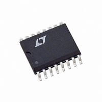
LTC1064-4CSW Linear Technology, LTC1064-4CSW Datasheet - Page 7

LTC1064-4CSW
Manufacturer Part Number
LTC1064-4CSW
Description
IC FILTR 8TH ORDR LOWPASS 16SOIC
Manufacturer
Linear Technology
Datasheet
1.LTC1064-4CSWPBF.pdf
(12 pages)
Specifications of LTC1064-4CSW
Filter Type
Cauer, Lowpass Switched Capacitor
Frequency - Cutoff Or Center
100kHz
Number Of Filters
1
Max-order
8th
Voltage - Supply
±2.375 V ~ 8 V
Mounting Type
Surface Mount
Package / Case
16-SOIC (0.300", 7.5mm Width)
Lead Free Status / RoHS Status
Contains lead / RoHS non-compliant
Other names
LTC1064-4CS
Available stocks
Company
Part Number
Manufacturer
Quantity
Price
Company:
Part Number:
LTC1064-4CSW
Manufacturer:
LT
Quantity:
106
Part Number:
LTC1064-4CSW
Manufacturer:
LT/凌特
Quantity:
20 000
Company:
Part Number:
LTC1064-4CSW#PBF
Manufacturer:
LTC
Quantity:
202
Company:
Part Number:
LTC1064-4CSW#PBF
Manufacturer:
LT
Quantity:
478
PI FU CTIO S
INV C, COMP1, INV A, COMP2 (Pins 1, 6, 7 and 13): To
obtain a Cauer response with minimum passband ripple
and cutoff frequencies above 20kHz, compensating com-
ponents are required. Figure 6 uses ±7.5V power supplies
and compensation components to achieve up to 40kHz
sweepable cutoff frequencies and ±0.1dB passband ripple.
Table 7 lists the typical amplitude response of Figure 6.
Figure 7 illustrates the compensation scheme required to
obtain a 100kHz cutoff frequency; Graph 4 and Tables 8
and 9 list the typical response of Figure 7 for 25°C and
125°C ambient temperature. As shown the ripple in-
creases at high temperatures but still a ±0.25dB figure
can be obtained for ambient temperatures below 70°C.
V
resistor tied to the inverting input of an op amp. Pin 2 is
protected against static discharge. The device’s output,
Pin 9, is the output of an op amp which can typically
source/sink 3mA/1mA. Although the internal op amps are
unity gain stable, driving long coax cables is not recom-
mended.
When testing the device for noise and distortion, the
output, Pin 9, should be buffered (Figure 4). The op amp
power supply wire (or trace) should be connected
directly to the power source. To eliminate any output
clock feedthrough, Pin 9 should be buffered with a simple
R, C lowpass filter (Figure 5). The cutoff frequency of the
output filter should be f
IN
U
, V
OUT
(Pins 2, 9): The input Pin 2 is connected to a 12k
U
U
CLK
(Pin Numbers Refer to the 14-Pin Package)
/3.
AGND (Pins 3, 5): For dual supply operation these pins
should be connected to a ground plane. For single supply
operation both pins should be tied to one half supply
(Figure 2).
V
capacitor to an adequate analog ground. Low noise,
nonswitching power supplies are recommended. To avoid
latchup when the power supplies exhibit high turn-on
transients, a 1N5817 Schottky diode should be added
from the V
INV A, R(h, I) (Pins 7, 14): A very short connection
between Pin 7 and Pin 14 is recommended. This connec-
tion should be preferably done under the IC package. In a
breadboard, use a one inch, or less, shielded coaxial cable;
the shield should be grounded. In a PC board, use a one
inch trace or less; surround the trace by a ground plane.
NC (Pin 8 ): Pin 8 is not internally connected, it should be
preferably grounded.
50/100 Ratio (Pin 10): For an f
Pin 10 should be tied to V
100:1, Pin 10 should be tied to V
midsupplies (i.e. ground), the filter response is neither
Cauer nor transitional. Table 6 illustrates this response.
Bypassing Pin 10 with a 0.1µF capacitor reduces the
already small clock feedthrough.
+
, V
–
(Pins 4, 12): Should be bypassed with a 0.1µF
+
and V
–
pins to ground (Figures 1 and 2).
+
. For an f
CLK
–
LTC1064-4
. When Pin 10 is at
/f
CLK
C
/f
ratio of 50:1,
–3dB
ratio of
10644fb
7


