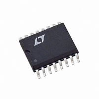
LTC1164-7CSW Linear Technology, LTC1164-7CSW Datasheet - Page 9

LTC1164-7CSW
Manufacturer Part Number
LTC1164-7CSW
Description
IC FILTR 8TH ORDR LOWPASS 16SOIC
Manufacturer
Linear Technology
Datasheet
1.LTC1164-7CSWPBF.pdf
(16 pages)
Specifications of LTC1164-7CSW
Filter Type
Linear Phase, Lowpass Switched Capacitor
Frequency - Cutoff Or Center
100kHz
Number Of Filters
1
Max-order
8th
Voltage - Supply
4.75 V ~ 16 V, ±2.375 V ~ 8 V
Mounting Type
Surface Mount
Package / Case
16-SOIC (0.300", 7.5mm Width)
Lead Free Status / RoHS Status
Contains lead / RoHS non-compliant
Other names
LTC1164-7CS
Available stocks
Company
Part Number
Manufacturer
Quantity
Price
Part Number:
LTC1164-7CSW
Manufacturer:
LINEAR/凌特
Quantity:
20 000
Company:
Part Number:
LTC1164-7CSW#PBF
Manufacturer:
Linear Technology
Quantity:
135
Company:
Part Number:
LTC1164-7CSW#PBF
Manufacturer:
LTC
Quantity:
90
PI FU CTIO S
NC (Pins 1, 8, 13): Pins 1, 8 and 13 are not connected to
any internal circuit point on the device and should be
preferably tied to analog ground.
Filter Input (Pin 2): The input pin is connected internally
through a 50k resistor tied to the inverting input of an op
amp.
Analog GND (Pins 3, 5): The filter performance depends
on the quality of the analog signal ground. For either dual
or single supply operation, an analog ground plane sur-
rounding the package is recommended. The analog ground
plane should be connected to any digital ground at a single
point. For dual supply operation, Pins 3 and 5 should be
connected to the analog ground plane. For single supply
operation, Pins 3 and 5 should be biased at 1/2 supply and
should be bypassed to the analog ground plane with at
least a 1µF capacitor (Figure 3). For single 5V operation at
the highest f
2V. This minimizes passband gain and phase variations.
Power Supply (Pins 4, 12): The V
12) should each be bypassed with a 0.1µF capacitor to an
adequate analog ground. The filter’s power supplies should
be isolated from other digital or high voltage analog
supplies. A low noise linear supply is recommended.
Using a switching power supply will lower the signal-to-
noise ratio of the filter. The supply during power-up should
have a slew rate less than 1V/µs. When V
V
should clamp V
typical connections for dual and single supply operation.
Filter Output (Pins 6, 9): Pin 6 is an intermediate filter
output providing an unspecified 6th order lowpass filter.
Pin 6 should not be loaded. Pin 9 is the specified output of
the filter; it can typically source/sink 1mA. Driving coaxial
cables or resistive loads less than 20k will degrade the
total harmonic distortion of the filter. When evaluating the
device’s distortion an output buffer is required. A
noninverting buffer, Figure 4, can be used provided that its
input common-mode range is well within the filter’s output
swing.
–
U
and V
–
U
is allowed to go above ground, a signal diode
CLK
–
of 2MHz, Pins 3 and 5 should be biased at
to prevent latch-up. Figures 2 and 3 show
U
+
(pin 4) and the V
+
is applied before
–
(Pin
External Connection (Pins 7, 14): Pins 7 and 14 should be
connected together. In a printed circuit board the connec-
tion should be done under the IC package through a short
trace surrounded by the analog ground plane.
Ratio Input (Pin 10): The DC level at this pin determines
the ratio of the clock frequency to the cutoff frequency of
the filter. Pin 10 at V
gives a 100:1 ratio. For single supply operation the ratio is
50:1 when Pin 10 is at V
ground. When Pin 10 is not tied to ground, it should be
bypassed to analog ground with a 0.1µF capacitor. If the
DC level at Pin 10 is switched mechanically or electrically
at slew rates greater than 1V/µs while the device is
operating, a 10k resistor should be connected between pin
10 and the DC source.
Clock Input (Pin 11): Any TTL or CMOS clock source with
a square-wave output and 50% duty cycle (±10%) is an
adequate clock source for the device. The power supply for
the clock source should not be the filter’s power supply.
The analog ground for the filter should be connected to
clock’s ground at a single point only. Table 7 shows the
clock’s low and high level threshold values for dual or
single supply operation. A pulse generator can be used as
a clock source provided the high level ON time is greater
than 0.5µs. Sine waves are not recommended for clock
input frequencies less than 100kHz, since excessively
slow clock rise or fall times generate internal clock jitter
(maximum clock rise or fall time ≤ 1µs). The clock signal
should be routed from the right side of the IC package and
perpendicular to it to avoid coupling to any input or output
analog signal path. A 1k resistor between clock source and
Pin 11 will slow down the rise and fall times of the clock to
further reduce charge coupling (Figures 2 and 3).
Table 7. Clock Source High and Low Threshold Levels
POWER SUPPLY
Dual Supply = ±7.5V
Dual Supply = ±5V
Dual Supply = ± 2.5V
Single Supply = 12V
Single Supply = 5V
+
gives a 50:1 ratio and pin 10 at V
+
and 100:1 when Pin 10 is at
HIGH LEVEL
≥ 2.18V
≥ 1.45V
≥ 0.73V
≥ 7.80V
≥ 1.45V
LTC1164-7
LOW LEVEL
≤ – 2.0V
≤ 0.5V
≤ 0.5V
≤ 6.5V
≤ 0.5V
11647fb
9
–


