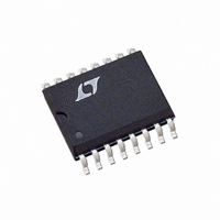
LTC1064-1CSW Linear Technology, LTC1064-1CSW Datasheet - Page 4

LTC1064-1CSW
Manufacturer Part Number
LTC1064-1CSW
Description
IC FILTR 8TH ORDR LOWPASS 16SOIC
Manufacturer
Linear Technology
Datasheet
1.LTC1064-1CNPBF.pdf
(8 pages)
Specifications of LTC1064-1CSW
Filter Type
Cauer, Lowpass Switched Capacitor
Frequency - Cutoff Or Center
50kHz
Number Of Filters
1
Max-order
8th
Voltage - Supply
±2.375 V ~ 8 V
Mounting Type
Surface Mount
Package / Case
16-SOIC (0.300", 7.5mm Width)
Lead Free Status / RoHS Status
Contains lead / RoHS non-compliant
Other names
LTC1064-1CS
Available stocks
Company
Part Number
Manufacturer
Quantity
Price
Company:
Part Number:
LTC1064-1CSW
Manufacturer:
LT
Quantity:
44
Part Number:
LTC1064-1CSW
Manufacturer:
LT
Quantity:
20 000
PI FU CTIO S
COMP1, INV A, COMP2, INV C (Pins 1,6,7, and 13): For
filter cutoff frequencies higher than 20kHz, in order to
minimize the passband ripple, compensation capacitors
should be added between Pin 6 and Pin 7 (COMP1) and
Pin 1 and Pin 13 (COMP2). For COMP1 (COMP2), add 1pF
(1.5pF) mica capacitor for each kHz increase in cutoff
frequency above 20kHz. For more detail refer to Gain vs
Frequency graphs.
V
18k resistor tied to the inverting input of an op amp. Pin 2
LTC1064-1
4
TYPICAL PERFOR A CE CHARACTERISTICS
–105
IN
–15
–30
–45
–60
–75
–90
15
U
, V
0
1
Gain vs Frequency
Typical Wideband Noise
(151µV
f
Grounded
OUT
CLK
V
T
A
S
= ±5V
= 25°C
= 1MHz, f
f
CLK
f
U
(Pins 2, 9): The input Pin 2 is connected to an
CLK
f
RMS
CLK
COMP1 NOT USED,
= 2MHz, f
= 3MHz, f
= 4MHz, f
FREQUENCY (kHz)
) V
COMP2 = 20pF
COMP1 = 24pF
COMP2 = 36pF
COMP1 = 36pF
COMP2 = 47pF
S
C
C
= ± 5V, T
C
= 10kHz Input
10
= 20kHz
U
= 30kHz
C
= 40kHz
A
(Pin Numbers Refer to the 14-Pin Package)
W
= 25°C
1064 G04
U
100
–105
–15
–30
–45
–60
–75
–90
15
0
Gain vs Frequency
1
Total Harmonic Distortion
(0.025%) V
f
Input = 1kHz at 3V
CLK
V
T
A
S
= ±7.5V
= 25°C
= 1MHz, f
f
CLK
f
CLK
f
CLK
FREQUENCY (kHz)
S
= 3MHz, f
= 4MHz, f
= 5MHz, f
= ± 7.5V, T
COMP1 = 10pF
C
COMP2 = 15pF
COMP1 = 20pF
COMP2 = 30pF
COMP1 = 30pF
COMP2 = 47pF
= 10kHz
10
is protected against static discharge. The device’s output,
Pin 9, is the output of an op amp which can typically source/
sink 3mA/1mA. Although the internal op amps are unity
gain stable, driving long coax cables is not recommended.
When testing the device for noise and distortion, the
output, Pin 9, should be buffered (Figure 4). The op amp
power supply wire (or trace) should be connected
directly to the power source.
AGND (Pins 3, 5): For dual supply operation these pins
should be connected to a ground plane. For single supply
RMS
C
C
C
= 30kHz
= 40kHz
= 50kHz
A
= 25°C
1064 G05
100
–10
–15
–20
–25
–30
–35
–5
48
44
40
36
32
28
24
20
16
12
5
0
8
4
0
0 2
1
Power Supply Current vs Power
Supply Voltage
Gain vs Frequency
V
f
f
COMP1 = 33pF
COMP2 = 56pF
f
CLK
C
CLK
S
= 50kHz
= ±7.5V
TOTAL POWER SUPPLY VOLTAGE (V)
= 5MHz
= 1MHz
4
6
25°C GAIN PEAK =
FREQUENCY (kHz)
8 10 12 14 16 18 20 22 24
0.4dB AT 30kHz
125°C GAIN PEAK =
10
1dB AT 35kHz
T
T
T
A
A
A
= –55°C
= 125°C
= 25°C
1064 G06
1064 G09
10641fa
100


