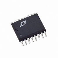
LTC1065CSW#TR Linear Technology, LTC1065CSW#TR Datasheet - Page 9

LTC1065CSW#TR
Manufacturer Part Number
LTC1065CSW#TR
Description
IC FILTER LP 5TH ORD LIN 16SOIC
Manufacturer
Linear Technology
Datasheet
1.LTC1065CSWPBF.pdf
(16 pages)
Specifications of LTC1065CSW#TR
Filter Type
Bessel, Lowpass Switched Capacitor
Frequency - Cutoff Or Center
50kHz
Number Of Filters
1
Max-order
5th
Voltage - Supply
±2.375 V ~ 8 V
Mounting Type
Surface Mount
Package / Case
16-SOIC (0.300", 7.5mm Width)
Architecture
Switched Capacitor
Order Filter (max)
5th
Single Supply Voltage (typ)
5/9/12/15V
Dual Supply Voltage (typ)
±5V
Power Supply Requirement
Single/Dual
Single Supply Voltage (min)
4.75V
Single Supply Voltage (max)
16V
Dual Supply Voltage (min)
±2.375V
Dual Supply Voltage (max)
±8V
Operating Temperature (min)
0C
Operating Temperature (max)
70C
Operating Temperature Classification
Commercial
Package Type
SOIC W
Lead Free Status / RoHS Status
Contains lead / RoHS non-compliant
Available stocks
Company
Part Number
Manufacturer
Quantity
Price
A
PPLICATI
0.80
0.75
0.70
0.65
0.60
0.55
0.50
0.45
0.40
0.80
0.75
0.70
0.65
0.60
0.55
0.50
0.45
0.40
–1
–2
–3
–4
4
3
2
1
0
0.5
0.5
0
Figure 5. f
C = 200pF
O
100
U
V
1.0
1.0
V
V
Figure 7. f
Figure 6. f
S
S
S
CLOCK FREQUENCY (MHz)
CLOCK FREQUENCY (MHz)
CLOCK FREQUENCY (kHz)
V
S
= ±2.5V
= ±2.5V
= ±2.5V
S
= ±2.5V
CLK
200
I FOR ATIO
1.5
1.5
U
T
vs Temperature
V
A
S
CLK
= –40°C
CLK
= ±7.5V
V
S
300
2.0
2.0
= ±7.5V
vs K
vs K
V
S
V
= ±5V
f
C = 10pF
T
f
C = 10pF
T
CLK
S
CLK
W
V
V
T
A
A
V
S
S
= ±5V
A
V
400
= 25°C
= 70°C
S
2.5
2.5
= ±7.5V
= 85°C
= ±7.5V
S
= K/RC
= K/RC
= ±5V
= ±5V
1065 F05
1065 F06
1065 F07
500
3.0
3.0
U
A 4pF parasitic capacitance is assumed in parallel with the
external 10pF capacitor. A ±1% clock frequency variation
from device to device can be expected. The 2MHz clock
frequency designed above will typically drift to 1.74MHz at
70°C (Figure 7).
The internal clock of the LTC1065 can be overridden by an
external clock provided that the external clock source can
drive the timing capacitor C, which is connected from the
clock input pin to ground.
Output Offset
The DC output offset of the LTC1065 is trimmed to
typically less than ±1mV. The trimming is done at V
±5V. To obtain optimum DC offset performance, appropri-
ate PC layout techniques should be used and the filter IC
should be soldered to the PC board. A socket will degrade
the output DC offset by typically 1mV. The output DC offset
is sensitive to the coupling of the clock output pin 4 (N
package) to the negative power supply pin 3 (N package).
The negative supply pin should be well decoupled. When
the surface mount package is used, all NC pins should be
grounded. When the output DC voltage is measured with
a voltmeter, the filter output pin should be buffered. Long
test leads should be avoided.
With fixed power supplies, the output DC offset should not
change by more than ±100µV over 10Hz to 1MHz clock
frequency variation. When the filter clock frequency is
fixed, the output DC offset will typically change by – 4mV
(2mV) when the power supply varies from ±5V to ±7.5V
(±2.5V). See Typical Performance Characteristics.
Common Mode Rejection
The common mode rejection is defined as the change of
the output DC offset with respect to the DC change of the
input voltage applied to the filter.
Table 3 illustrates the common mode rejection for three
power supplies and three temperatures. The common
mode rejection improves if the output offset is adjusted to
approximately 0V. The output offset can be adjusted via
pin 8 (N package). See Typical Applications.
CMR = 20log (∆V
OS OUT
/∆V
IN
)(dB)
LTC1065
1065fb
9
S
=


