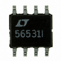
LTC1565-31IS8#TR Linear Technology, LTC1565-31IS8#TR Datasheet - Page 3

LTC1565-31IS8#TR
Manufacturer Part Number
LTC1565-31IS8#TR
Description
IC FILTR 7TH ORDER 650KHZ 8-SOIC
Manufacturer
Linear Technology
Datasheet
1.LTC1565-31CS8PBF.pdf
(12 pages)
Specifications of LTC1565-31IS8#TR
Filter Type
Linear Phase, Continuous-Time Lowpass
Frequency - Cutoff Or Center
650kHz
Number Of Filters
1
Max-order
7th
Voltage - Supply
4.75 V ~ 11 V, ±4.75 V ~ 5.5 V
Mounting Type
Surface Mount
Package / Case
8-SOIC (3.9mm Width)
Dual Supply Voltage (typ)
±3/±5V
Power Supply Requirement
Single/Dual
Single Supply Voltage (min)
4.75V
Dual Supply Voltage (min)
±2.375V
Operating Temperature (min)
-40C
Operating Temperature (max)
85C
Lead Free Status / RoHS Status
Contains lead / RoHS non-compliant
Other names
LTC1565-31IS8TR
Available stocks
Company
Part Number
Manufacturer
Quantity
Price
ELECTRICAL CHARACTERISTICS
PARAMETER
Input Bias Current
Input Offset Current
Input Resistance
Input Capacitance
Output DC Offset (Note 3)
Output DC Offset Drift
Ground Voltage (Pin 3) in
Single Supply Applications
SHDN Pin Logic Thresholds
SHDN Pin Pull-Up Current
Power Supply Current
Power Supply Current in Shutdown Mode
Note 1: Stresses beyond those listed under Absolute Maximum Ratings
may cause permanent damage to the device. Exposure to any Absolute
Maximum Rating condition for extended periods may affect device
reliability and lifetime.
Note 2: Input and output voltages expressed as peak-to-peak numbers are
assumed to be fully differential.
TYPICAL PERFORMANCE CHARACTERISTICS
temperature range, otherwise specifi cations are at T
unless otherwise specifi ed.
–100
–10
–20
–30
–40
–50
–60
–70
–80
–90
10
0
10
Frequency Response
4
10
FREQUENCY (Hz)
DELAY
5
GAIN
10
CONDITIONS
Common Mode, V
Differential
V
V
V
V
V
V
V
V
V
V
V
V
V
Shutdown. Includes SHDN Pull-Up Current
S
S
S
S
S
S
S
S
S
S
S
S
S
6
V
V
= 5V
= ±5V (Note 5)
= 5V
= ±5V
= 5V
= 5V, Minimum Logical “1”
= 5V, Maximum Logical “0”
= ±5V, Minimum Logical “1”
= ±5V, Maximum Logical “0”
= 5V
= ±5V
= 5V
= ±5V
S
S
= 5V
= ±5V
1565 G01
A
10
= 25°C. V
7
2.0
1.9
1.8
1.7
1.6
1.5
1.4
1.3
1.2
1.1
1.0
0.9
The
IN
= 2.5V
l
S
denotes the specifi cations which apply over the full operating
= 5V, R
Note 3: Output DC offset is measured between Pin 8 and Pin 7 with Pin 1
and Pin 2 connected to Pin 3.
Note 4: Thermal resistance varies depending upon the amount of PC board
metal attached to the device. θ
board covered with 2 oz copper on both sides.
Note 5: Output DC offset measurements are performed by automatic test
equipment approximately 0.5 seconds after application of power.
LOAD
= 10k from each output to AC ground, and Pin 5 open
–0.5
–1.0
–1.5
–2.0
–2.5
–3.0
–3.5
–4.0
–4.5
0.5
0
25k
Passband Gain and Delay
vs Frequency
T
A
= 25°C
FREQUENCY (Hz)
100k
l
l
l
l
l
l
l
l
l
JA
DELAY
GAIN
is specifi ed for a 3.8 square inch test
2.49
MIN
0.1
3.3
2.4
5V
LTC1565-31
±5V
–400
–400
2.51
TYP
±10
145
0.3
75
±5
±5
24
25
20
3
5
9
8
1565 G02
1M
2.0
1.9
1.8
1.7
1.6
1.5
1.4
1.3
1.2
1.1
1.0
MAX
2.52
±12
±12
0.6
4.2
2.9
31
33
16
40
156531fa
UNITS
μV/°C
μV/°C
3
MΩ
MΩ
mV
mV
mA
mA
μA
nA
μA
μA
μA
μA
pF
V
V
V
V
V


