MF10CCN/NOPB National Semiconductor, MF10CCN/NOPB Datasheet - Page 4
MF10CCN/NOPB
Manufacturer Part Number
MF10CCN/NOPB
Description
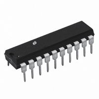
IC FILTER DUAL SWITCH CAP 20-DIP
Manufacturer
National Semiconductor
Datasheet
1.MF10CCWMNOPB.pdf
(28 pages)
Specifications of MF10CCN/NOPB
Filter Type
Universal Switched Capacitor
Frequency - Cutoff Or Center
200kHz
Number Of Filters
2
Max-order
4th
Voltage - Supply
±9 V ~ 14 V
Mounting Type
Through Hole
Package / Case
20-DIP (0.300", 7.62mm)
Ic Filter Type
Switched Capacitor
Filter Order
4th
No. Of Filters
2
Cutoff Frequency
30kHz
Program Clock Frequency Typ
1.5MHz
Supply Voltage Range
± 9V To ± 14V
Rohs Compliant
Yes
Lead Free Status / RoHS Status
Lead free / RoHS Compliant
Other names
*MF10CCN
*MF10CCN/NOPB
MF10
MF10CCN
MF10CN
*MF10CCN/NOPB
MF10
MF10CCN
MF10CN
Available stocks
Company
Part Number
Manufacturer
Quantity
Price
Company:

Part Number:
MF10CCN/NOPB
Manufacturer:
NSC
Quantity:
1 267


www.national.com
Logic Input Characteristics
Note 1: Absolute Maximum Ratings indicate limits beyond which damage to the device may occur. DC and AC electrical specifications do not apply when operating
the device beyond its specified operating conditions.
Note 2: When the input voltage (V
to 5 mA or less. The 20 mA package input current limits the number of pins that can exceed the power supply boundaries with a 5 mA current limit to four.
Note 3: The maximum power dissipation must be derated at elevated temperatures and is dictated by T
allowable power dissipation at any temperature is P
T
increases to 95˚C/W and for the MF10ACWM/CCWM this number is 66˚C/W.
Note 4: The accuracy of the Q value is a function of the center frequency (f
Characteristics”.
Note 5: V
Note 6: For
the MF10 with a 50:1 CLK ratio and 280 µV rms for the MF10 with a 100:1 CLK ratio.
Note 7: The short circuit source current is measured by forcing the output that is being tested to its maximum positive voltage swing and then shorting that output
to the negative supply. The short circuit sink current is measured by forcing the output that is being tested to its maximum negative voltage swing and then shorting
that output to the positive supply. These are the worst case conditions.
Note 8: Typicals are at 25˚C and represent most likely parametric norm.
Note 9: Tested limits are guaranteed to National’s AOQL (Average Outgoing Quality Level).
Note 10: Design limits are guaranteed but not 100% tested. These limits are not used to calculate outgoing quality levels.
Note 11: Human body model, 100 pF discharged through a 1.5 k
JMAX
Boldface limits apply for T
= 125˚C, and the typical junction-to-ambient thermal resistance of the MF10ACN/CCN when board mounted is 55˚C/W. For the MF10AJ/CCJ, this number
OS1
±
, V
5V supplies the dynamic range is referenced to 2.82V rms (4V peak) where the wideband noise over a 20 kHz bandwidth is typically 200 µV rms for
OS2
Parameter
, and V
Min Logical “1”
Max Logical “0”
OS3
refer to the internal offsets as discussed in the Applications Information Section 3.4.
IN
) at any pin exceeds the power supply rails (V
MIN
to T
MAX
D
= (T
; all other limits T
V
V
JMAX
+
LSh
(Continued)
= +10V, V
− T
Conditions
= 0V
A
)/
resistor.
JA
or the number given in the Absolute Maximum Ratings, whichever is lower. For this device,
−
A
= 0V,
= T
4
O
IN
J
). This is illustrated in the curves under the heading “Typical Performance
= 25˚C
<
V
−
or V
(Note 8)
Typical
IN
>
V
+
) the absolute value of current at that pin should be limited
JMAX
MF10ACN, MF10CCN,
,
JA
MF10CCWM
, and the ambient temperature, T
(Note 9)
Tested
Limit
+2.0
+0.8
(Note 10)
Design
Limit
+2.0
+0.8
A
. The maximum
Units
V
V
Related parts for MF10CCN/NOPB
Image
Part Number
Description
Manufacturer
Datasheet
Request
R

Part Number:
Description:
IC, FILTER DUAL SWITCHED CAP, DIP20
Manufacturer:
National Semiconductor
Datasheet:
Part Number:
Description:
National Semiconductor [8-Bit D/A Converter]
Manufacturer:
National Semiconductor
Datasheet:
Part Number:
Description:
National Semiconductor [Media Coprocessor]
Manufacturer:
National Semiconductor
Datasheet:
Part Number:
Description:
Digitally Controlled Tone and Volume Circuit with Stereo Audio Power Amplifier, Microphone Preamp Stage and National 3D Sound
Manufacturer:
National Semiconductor
Datasheet:
Part Number:
Description:
Digitally Controlled Tone and Volume Circuit with Stereo Audio Power Amplifier, Microphone Preamp Stage and National 3D Sound
Manufacturer:
National Semiconductor
Datasheet:
Part Number:
Description:
AC97 Rev 2 Codec with Sample Rate Conversion and National 3D Sound
Manufacturer:
National Semiconductor
Part Number:
Description:
Manufacturer:
National Semiconductor
Datasheet:
Part Number:
Description:
Manufacturer:
National Semiconductor
Datasheet:
Part Number:
Description:
General Purpose, Low Voltage, Low Power, Rail-to-Rail Output Operational Amplifiers
Manufacturer:
National Semiconductor
Datasheet:
Part Number:
Description:
8-bit 20 MSPS flash A/D converter.
Manufacturer:
National Semiconductor
Datasheet:
Part Number:
Description:
Low Noise Quad Operational Amplifier
Manufacturer:
National Semiconductor
Datasheet:
Part Number:
Description:
Quad Differential Line Receivers
Manufacturer:
National Semiconductor
Datasheet:
Part Number:
Description:
Quad High Speed Trapezoidal? Bus Transceiver
Manufacturer:
National Semiconductor
Datasheet:
Part Number:
Description:
Dual Line Receiver
Manufacturer:
National Semiconductor
Datasheet: