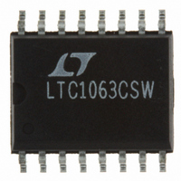
LTC1063CSW Linear Technology, LTC1063CSW Datasheet - Page 9

LTC1063CSW
Manufacturer Part Number
LTC1063CSW
Description
IC FILTR 5TH ORDER LOWPASS16SOIC
Manufacturer
Linear Technology
Datasheet
1.LTC1063CN8PBF.pdf
(16 pages)
Specifications of LTC1063CSW
Filter Type
Butterworth, Lowpass Switched Capacitor
Frequency - Cutoff Or Center
50kHz
Number Of Filters
1
Max-order
5th
Voltage - Supply
±2.375 V ~ 8 V
Mounting Type
Surface Mount
Package / Case
16-SOIC (0.300", 7.5mm Width)
Lead Free Status / RoHS Status
Contains lead / RoHS non-compliant
Other names
LTC1063CS
Available stocks
Company
Part Number
Manufacturer
Quantity
Price
Part Number:
LTC1063CSW#PBF
Manufacturer:
LINEAR/凌特
Quantity:
20 000
APPLICATIO S I FOR ATIO
Self-Clocking Operation
The LTC1063 features an internal oscillator which can be
tuned via an external RC. The LTC1063’s internal oscillator
is primarily intended for generation of clock frequencies
below 500kHz. The first curve of the Typical Performance
Characteristics section shows how to quickly choose the
value of the RC for a given frequency. More precisely, the
frequency of the internal oscillator is equal to:
For clock frequencies (f
Figure 4b shows the variation of the parameter K versus
clock frequency and power supply. First choose the de-
sired clock frequency, (f
Figure 4b pick the right value of K, set C = 200pF and solve
for R.
Example 1: f
then,
f
CLK
= K/RC
1.25
1.20
1.15
1.10
1.05
1.00
0.95
0.90
0.85
0.80
0.75
T
R = (1.0)/(200kHz × 204pF) = 24.5k.
CUTOFF
A
= 25°C, K = 1.0, C = 200pF
F
C = 200pF
T
100
CLK
A
V
INTERNAL CLOCK FREQUENCY (kHz)
= 25°C
V
IN
–
= K/RC
U
Figure 4b. f
= 2kHz, f
1
2
3
4
200
CLK
Figure 4a.
LTC1063
V
V
U
S
S
CLK
) below 100kHz, K equals 1.07.
= ±7.5V
= ±2.5V
R
300
CLK
CLK
< 500kHz), then through
= 200kHz, V
vs K
400
8
7
6
5
V
W
S
= ±5V
V
V
OUT
+
C
500
1063 F04b
1063 F04a
S
U
= ±5V,
For a very limited temperature range, the internal oscillator
of the LTC1063 can be used to generate clock frequencies
above 500kHz (Figures 6 and 7). The data of Figure 6 is
derived from several devices. For a given external (RC)
value, the observed device-to-device clock frequency varia-
tion was ±1% (V
Example 2:
from Figure 6, K = 0.575,
and,
Note a 4pF parasitic capacitance is assumed in parallel
with the external 200pF timing capacitor. Figure 5 shows
the clock frequency variation from – 40°C to 85°C. The
200kHz clock of Example 1 will change by –1.75% at 85°C.
0.80
0.75
0.70
0.65
0.60
0.55
0.50
0.45
0.40
–1
–2
–3
–4
4
3
2
1
0
0.5
0
f
T
R = (0.575)/(2MHz × 14pF) = 20.5k.
C = 200pF
CUTOFF
Figure 5. f
A
S
= 25°C, C = 10pF
= ±5V), and ±1.25% for V
100
1.0
V
V
S
S
Figure 6. f
CLOCK FREQUENCY (MHz)
CLOCK FREQUENCY (kHz)
V
= ±2.5V
= ±2.5V
S
= 20kHz, f
= ±2.5V
200
CLK
1.5
T
A
vs Temperature
= –40°C
V
CLK
S
300
2.0
= ±7.5V
CLK
vs K
V
f
C = 10pF
T
S
CLK
V
V
A
T
V
= 2MHz, V
= ±5V
S
S
A
400
V
= 25°C
2.5
S
S
= ±7.5V
= 85°C
= ±7.5V
= K/RC
= ±5V
= ±5V
1063 F05
1063 F06
LTC1063
500
3.0
S
= ±2.5V.
S
= ±7.5V,
1063fa
9


