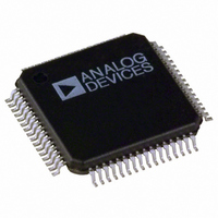
ADV7191KSTZ Analog Devices Inc, ADV7191KSTZ Datasheet - Page 43

ADV7191KSTZ
Manufacturer Part Number
ADV7191KSTZ
Description
IC ENCODER VIDEO W/DAC 64LQFP
Manufacturer
Analog Devices Inc
Type
Video Encoderr
Datasheet
1.ADV7191KST.pdf
(72 pages)
Specifications of ADV7191KSTZ
Applications
DVD, PC Video, Multimedia
Voltage - Supply, Analog
3.3 V ~ 5 V
Mounting Type
Surface Mount
Package / Case
64-LQFP
Number Of Dac's
6
Adc/dac Resolution
10b
Screening Level
Commercial
Package Type
LQFP
Pin Count
64
Lead Free Status / RoHS Status
Lead free / RoHS Compliant
Voltage - Supply, Digital
-
Lead Free Status / RoHS Status
Compliant, Lead free / RoHS Compliant
Available stocks
Company
Part Number
Manufacturer
Quantity
Price
Company:
Part Number:
ADV7191KSTZ
Manufacturer:
FUJITSU
Quantity:
92
Part Number:
ADV7191KSTZ
Manufacturer:
ADI/亚德诺
Quantity:
20 000
BRIGHTNESS DETECT REGISTER
(Address (SR5–SR0) = 34H)
T
to read back data in order to monitor the brightness/darkness of
the incoming video data on a field-by-field basis. The brightness
information is read from the I
the color controls or the gamma correction controls may be
adjusted.
The luma data is monitored in the active video area only. The
average brightness I
every VSYNC signal.
O
(Address (SR4–SR0) = 35H)
T
87 shows the various operations under the control of this register.
REV. B
he Brightness Detect Register is an 8-bit-wide register used only
he Output Clock Register is an 8-bit-wide register. Figure
UTPUT CLOCK REGISTER (OCR 9–0)
2
C register is updated on the falling edge of
ZERO MUST BE
WRITTEN TO
THIS BIT
OCR07
OCR07
2
C and based on this information,
OCR06
Figure 87. Output Clock Register (OCR)
OCR06 – OCR04
ONE MUST BE
WRITTEN TO
THESE BITS
OCR05
OCR04
–43–
OCR03
O
Reserved (OCR00)
A Logic 0 must be written to this bit.
CLKOUT Pin Control (OCR01)
This bit enables the CLKOUT pin when set to 1 and, therefore,
outputs a 54 MHz clock generated by the internal PLL. The
PLL and 4¥ Oversampling have to be enabled for this control to
take effect (MR61 = 0; MR16 = 1).
Reserved (OCR02–03)
A Logic 0 must be written to these bits.
Reserved (OCR04–06)
A Logic 1 must be written to these bits.
Reserved (OCR07)
A Logic 0 must be written to this bit.
ZERO MUST BE
OCR03 – OCR02
CR BIT DESCRIPTION
WRITTEN TO
THESE BITS
OCR02
OCR01
0
1
PIN CONTROL
CLKOUT
OCR01
DISABLED
ENSABLED
ZERO MUST BE
WRITTEN TO
THIS BIT
OCR00
OCR00
ADV7190/ADV7191


