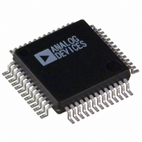
ADV7195KS Analog Devices Inc, ADV7195KS Datasheet - Page 11

ADV7195KS
Manufacturer Part Number
ADV7195KS
Description
IC DAC VID-HDTV 3CH-11BIT 52MQFP
Manufacturer
Analog Devices Inc
Type
Video Encoderr
Datasheet
1.ADV7195KS.pdf
(36 pages)
Specifications of ADV7195KS
Rohs Status
RoHS non-compliant
Applications
HDTV, MPEG, Image Processing
Voltage - Supply, Analog
3.3V
Voltage - Supply, Digital
3.3V
Mounting Type
Surface Mount
Package / Case
52-MQFP, 52-PQFP
Adc/dac Resolution
11b
Screening Level
Commercial
Package Type
MQFP
Pin Count
52
For Use With
EVAL-ADV7195EB - BOARD EVAL FOR ADV7195
Lead Free Status / RoHS Status
Not Compliant
Available stocks
Company
Part Number
Manufacturer
Quantity
Price
Part Number:
ADV7195KSZ
Manufacturer:
ADI/亚德诺
Quantity:
20 000
PROGRAMMABLE ADAPTIVE FILTER CONTROL
If the Adaptive Filter Mode is enabled (Progressive Scan Mode
only), it is possible to compensate for large edge transitions on
the incoming Y data. Sensitivity and attenuation are all pro-
grammable over the I
Sharpness Filter Control and Adaptive Filter Control section.
INPUT/OUTPUT CONFIGURATION
Table I shows possible input/output configurations when using
the ADV7195.
–80
–10
–20
–30
–40
–50
–60
–70
–10
–20
–30
–40
–50
–60
–70
–80
10
10
0
0
0
0
Input Format
YCrCb Progressive Scan
YCrCb HDTV
RGB Progressive Scan
RGB HDTV
Async Timing Mode
4:2:2
4:4:4
4:2:2
4:4:4
4:4:4
4:4:4
All Inputs
5
5
×
2
C. For further information refer to
10
10
Table I.
15
15
20
20
Output
2×
1× or 2×
1×
1×
2×
1×
1×
25
25
30
30
MPU PORT DESCRIPTION
The ADV7195 support a 2-wire serial (I
processor bus driving multiple peripherals. Two inputs, Serial
Data (SDA) and Serial Clock (SCL) carry information between
any device connected to the bus. Each slave device is recognized
by a unique address. The ADV7195 has four possible slave
addresses for both read and write operations. These are unique
addresses for each device and are illustrated in Figure 11. The
LSB sets either a read or write operation. Logic Level “1” corre-
sponds to a read operation while Logic Level “0” corresponds to
a write operation. A1 is set by setting the ALSB pin of the
ADV7195 to Logic Level “0” or Logic Level “1.” When ALSB is
set to “0,” there is greater input bandwidth on the I
which allows high-speed data transfers on this bus. When ALSB
is set to “1,” there is reduced input bandwidth on the I
lines, which means that pulses of less than 50 ns will not pass
into the I
for noisy systems.
To control the various devices on the bus the following protocol
must be followed. First the master initiates a data transfer by
establishing a Start condition, defined by a high-to-low transi-
tion on SDA while SCL remains high. This indicates that an
address/data stream will follow. All peripherals respond to the
Start condition and shift the next eight bits (7-bit address + R/W
bit). The bits are transferred from MSB down to LSB. The
peripheral that recognizes the transmitted address responds by
pulling the data line low during the ninth clock pulse. This is
known as an acknowledge bit. All other devices withdraw from
the bus at this point and maintain an idle condition. The idle
condition is where the device monitors the SDA and SCL lines
waiting for the Start condition and the correct transmitted
address. The R/W bit determines the direction of the data.
1
–80
–10
–20
–30
–40
–50
–60
–70
10
0
2
0
C internal controller. This mode is recommended
1
5
0
10
1
15
0
2
20
C-compatible) micro-
1
SETUP BY
ADDRESS
CONTROL
ADV7195
ALSB
A1
25
READ/WRITE
0
1
2
CONTROL
C lines,
X
30
WRITE
READ
2
C


