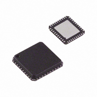
ADV7179BCP Analog Devices Inc, ADV7179BCP Datasheet - Page 7

ADV7179BCP
Manufacturer Part Number
ADV7179BCP
Description
IC ENCODER VID NTSC/PAL 40LFCSP
Manufacturer
Analog Devices Inc
Type
Video Encoderr
Datasheet
1.ADV7179KCPZ.pdf
(52 pages)
Specifications of ADV7179BCP
Rohs Status
RoHS non-compliant
Applications
Digital Cameras, Mobile Phones, Portable Video
Voltage - Supply, Analog
2.8 V, 3.3 V
Mounting Type
Surface Mount
Package / Case
40-LFCSP
Adc/dac Resolution
10b
Screening Level
Industrial
Package Type
LFCSP EP
Pin Count
40
Voltage - Supply, Digital
-
Lead Free Status / RoHS Status
Not Compliant
Available stocks
Company
Part Number
Manufacturer
Quantity
Price
Company:
Part Number:
ADV7179BCP
Manufacturer:
ADI
Quantity:
455
Company:
Part Number:
ADV7179BCPZ
Manufacturer:
ADI
Quantity:
230
Part Number:
ADV7179BCPZ
Manufacturer:
ADI/亚德诺
Quantity:
20 000
Company:
Part Number:
ADV7179BCPZ-REEL
Manufacturer:
XILINX
Quantity:
1 150
3.3 V TIMING SPECIFICATIONS
V
Table 4.
Parameter
MPU PORT
ANALOG OUTPUTS
CLOCK CONTROL AND PIXEL PORT
TELETEXT
RESET CONTROL
1
2
3
4
5
6
The maximum/minimum specifications are guaranteed over this range. The maximum/minimum values are typical over 3.0 V to 3.6 V range.
Temperature range T
TTL input values are 0 V to 3 V, with input rise/fall times −3 ns, measured between the 10% and 90% points. Timing reference points at 50% for inputs and outputs.
Analog output load –10 pF.
Guaranteed by characterization.
Output delay measured from the 50% point of the rising edge of CLOCK to the 50% point of full-scale transition.
See Figure 60.
AA
SCLOCK Frequency
SCLOCK High Pulse Width, t
SCLOCK Low Pulse Width, t
Hold Time (Start Condition), t
Setup Time (Start Condition), t
Data Setup Time, t
SDATA, SCLOCK Rise Time, t
SDATA, SCLOCK Fall Time, t
Setup Time (Stop Condition), t
Analog Output Delay
DAC Analog Output Skew
f
Clock High Time, t
Clock Low Time, t
Data Setup Time, t
Data Hold Time, t
Control Setup Time, t
Control Hold Time, t
Digital Output Access Time, t
Digital Output Hold Time, t
Pipeline Delay, t
Digital Output Access Time, t
Data Setup Time, t
Data Hold Time, t
RESET Low Time
CLOCK
= 3.0 V–3.6 V
3, 4
3, 4
, 3 4
MIN
1
PD
3, 5
, V
12
18
10
6
9
5
11
17
to T
REF
12
11
MAX
= 1.235 V, R
: –40°C to +85°C.
14
2
7
1
6
13
16
3
4
8
4, 5
SET
= 150 Ω. All specifications T
Conditions
After this period, the first clock is generated
Relevant for repeated start condition
1
Rev. B | Page 7 of 52
MIN
to T
MAX
2
, unless otherwise noted.
Min
0
0.6
1.3
0.6
0.6
100
0.6
8
8
3.5
4
4
3
6
Typ
7
0
27
12
8
48
23
2
6
ADV7174/ADV7179
Max
400
300
300
Unit
kHz
μs
μs
μs
μs
ns
ns
ns
μs
ns
ns
MHz
ns
ns
ns
ns
ns
ns
ns
ns
Clock Cycles
ns
ns
ns
ns


