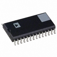
AD1892JRRL Analog Devices Inc, AD1892JRRL Datasheet - Page 17

AD1892JRRL
Manufacturer Part Number
AD1892JRRL
Description
IC SAMPLE CONV W/RX 20BIT 28SOIC
Manufacturer
Analog Devices Inc
Type
Sample Rate Converterr
Datasheet
1.AD1892JR.pdf
(24 pages)
Specifications of AD1892JRRL
Rohs Status
RoHS non-compliant
Applications
Players, Recorders
Voltage - Supply, Digital
4.5 V ~ 5.5 V
Mounting Type
Surface Mount
Package / Case
28-SOIC (7.5mm Width)
Voltage - Supply, Analog
-
REV. 0
The incoming 16-bit CRC Word (Q82 through Q97) is routed
to the AD1892 CRC circuit block. The CRC block generates
a 16-bit polynomial against the first 80 bits of the incoming
Q-channel subcode and flags a CRC error if the generated CRC
is different from the incoming CRC (Q82 through Q97). Q-
Channel CRC errors are flagged in the AD1892 Status Register
1 in position D6.
An external microcontroller or microprocessor can use the
QDFS (Pin 6) output from the AD1892 as an interrupt to alert
the microcontroller that a new Q-Channel block is ready. When
the input sample rate is 44.1 kHz, the QDFS frequency is 75 Hz
([44,100
OPERATING ISSUES
Serial Data Output Port
The AD1892 uses the frequency of the master clock (MCLK,
Pin 28) to determine the output sample rate. The LRCLK
signal is divided down from the master clock by a factor of 512.
The phase of this division can be adjusted by using the sync
input pin. The AD1892 is a clock master device; the audio data
clocks, bit clock (BCLK, Pin 26) and left/right clock are outputs
only. LRCLK runs continuously and transitions twice per stereo
sample period. BCLK also runs continuously and is used only to
clock the audio data from the AD1892’s serial data output port.
The AD1892’s flexible serial data output port transmits data in
twos-complement, MSB-first format. The left channel data
field always precedes the right channel data field. The output
data consists of 16 or 20 bits as established by settings in Con-
trol Register 1 (Bit D5). The BCLK frequency can be set
to either 32
Control Register 1.
OUTPUT
OUTPUT
OUTPUT
LRCLK
SDATA
BCLK
OUTPUT
OUTPUT
OUTPUT
OUTPUT
OUTPUT
OUTPUT
SDATA
SDATA
LRCLK
LRCLK
BCLK
BCLK
LSB
2]/1176 = 75).
F
SOUT
MSB
MSB–1 MSB–2
or 64
MSB
MSB–1 MSB–2
F
SOUT
MSB
(default) using Bit D1 in
LEFT CHANNEL
LEFT CHANNEL
LSB+2 LSB+1
MSB–1 MSB–2
LSB+2
LEFT CHANNEL
LSB+1
LSB
Figure 27. Right-Justified Mode
Figure 29. Left-Justified Mode
Figure 28. I
LSB
LSB+2
LSB+1
2
–17–
S-Justified Mode
LSB
Serial Output Port Modes
The AD1892 uses two bits in Control Register 1 to control the
mode configuration of the output data port. Bits D4 and D3
program the output data port mode as shown in Table III.
D4 D3
LO LO
LO HI
HI
HI
Note that in all three modes, the AD1892 is a “master” device,
i.e., the LRCLK, the BCLK and the SDATA signals are always
outputs. This is also true in bypass mode.
Figure 27 shows the right-justified mode. LRCLK is HI for the
left channel and LO for the right channel. Data is valid on the
rising edge of BCLK. The MSB is delayed 12-bit clock periods
(in 20-bit output mode) or 16-bit clock periods (in 16-bit out-
put mode) from an LRCLK transition, so that when there are
64 BCLK periods per LRCLK period, the LSB of the data will
be right-justified to the next LRCLK transition.
Figure 28 shows the default I
is used without a supporting microcontroller or microprocessor,
it will default to the I
LO for the left channel and HI for the right channel. Data is
valid on the rising edge of BCLK. The MSB is left-justified to
an LRCLK transition but with a single BCLK period delay. The
I
output mode.
Figure 29 shows the left-justified mode. LRCLK is HI for the
left channel and LO for the right channel. Data is valid on the
rising edge of BCLK. The MSB is left-justified to an LRCLK
transition with no MSB delay. The left-justified mode can be
used in the 16-bit or 20-bit output mode.
MSB
2
S-justified mode can be used in either the 16-bit or the 20-bit
MSB–1 MSB–2
MSB
LO
HI
Table III. Serial Output Port Mode Control Bits
MSB–1 MSB–2
Serial Output Port Mode
I
Left-Justified (See Figure 29)
Right-Justified (See Figure 27)
Reserved
2
S-Justified (See Figure 28) Default
RIGHT CHANNEL
RIGHT CHANNEL
2
LSB+2
S-justified mode after reset. LRCLK is
MSB
MSB–1 MSB–2
RIGHT CHANNEL
LSB+2 LSB+1
LSB+1
2
S-justified mode. When the AD1892
LSB
LSB
LSB+2
LSB+1
AD1892
LSB
MSB
MSB+1
MSB


