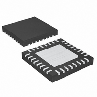
MAX9526ATJ+ Maxim Integrated Products, MAX9526ATJ+ Datasheet - Page 31

MAX9526ATJ+
Manufacturer Part Number
MAX9526ATJ+
Description
IC VID DECODER NTSC/PAL 32-TQFN
Manufacturer
Maxim Integrated Products
Type
Video Decoderr
Datasheet
1.MAX9526AEI.pdf
(38 pages)
Specifications of MAX9526ATJ+
Applications
Automotive Systems, Players, TV
Voltage - Supply, Analog
1.8V
Voltage - Supply, Digital
1.8V
Mounting Type
Surface Mount
Package / Case
32-TQFN Exposed Pad
Lead Free Status / RoHS Status
Lead free / RoHS Compliant
1 = Clip ITU output to Y range is between 64–940 and
0 = Clip ITU output to Y range and CbCr range is
This signal inverts the polarity of the line-locked clock
that is output from the MAX9526. This can be used to
solve board level timing problems for other devices.
1 = Invert LLC clock.
0 = Do not invert LLC clock (default).
1 = 54MHz clock at XTAL/OSC input.
0 = 27MHz clock at XTAL/OSC input (default).
This bit is only applicable when the crystal oscillator is
disabled (XTAL_DIS = 1).
1 = XTAL/OSC is either a 27MHz or a 54MHz CMOS
0 = Enables the 27MHz crystal oscillator (default).
1 = D1 and D0 output horizontal and vertical sync
0 = D1 and D0 are LSBs of digital component video
The rising edge of horizontal sync (HS) coincides with
the end of active video (rises after 3FFh 000h of EAV
code). The falling edge coincides with the start of
Clock and Output Control Register
between 5–1019 (default).
CbCr range is between 64–960.
pulses, respectively.
0x0D
output (default).
REG
clock input.
ITU-R BT.656 Standard Clipping Level (CLIP)
Input Clock Frequency Select (SEL_54MHz)
Horizontal/Vertical Sync Output (HSVS)
Inverted Line-Locked Clock (LLC_INV)
Crystal Oscillator Disable (XTAL_DIS)
______________________________________________________________________________________
B7
0
CLIP
B6
LLC_INV
Low-Power, High-Performance
B5
SEL_54MHZ
NTSC/PAL Video Decoder
B4
active video (SAV) code (falls after completing 3FFh
000h of SAV code). Figure 18 shows the horizontal and
vertical sync timing.
The vertical sync pulse (VS) line transitions are detailed
in Table 8. Note that the VS line transitions on pin D0
are shifted by 1 to 2 lines relative to the V flag transi-
tions embedded in the ITU data stream. The V flag tran-
sitions embedded in the ITU data stream follow the
ITU-R BT.656-4 standard.
1 = Logic data outputs (D9–D0) are disabled and
0 = Logic data outputs (D9–D0) are enabled (default).
The DATAZ bit forces data outputs high impedance
regardless of whether the device is in shutdown.
1 = Logic clock output (LLC) is disabled and placed
0 = Logic clock output (LLC) is enabled (default).
The LLCZ bit forces LLC high impedance regardless of
whether the device is in shutdown.
Table 8. VS (Pin D0) Line Transitions
Field 1
Field 2
VERTICAL SYNC PULSES
in a high-impedance state.
placed in high-impedance state.
XTAL_DIS
(VS on Pin D0)
B3
Start (VS = 1)
Finish (VS = 0)
Start (VS = 1)
Finish (VS = 0)
HSVS
B2
Data Output Disable (DATAZ)
Clock Output Disable (LLCZ)
Line 623
Line 309
Line 335
DATAZ
Line 21
B1
625
Line 265
Line 284
Line 21
LLCZ
Line 2
525
B0
31


