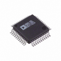
ADV7177KSZ Analog Devices Inc, ADV7177KSZ Datasheet - Page 26

ADV7177KSZ
Manufacturer Part Number
ADV7177KSZ
Description
IC DAC VIDEO NTSC 3-CH 44MQFP
Manufacturer
Analog Devices Inc
Type
Video Encoderr
Datasheet
1.ADV7177KSZ-REEL.pdf
(44 pages)
Specifications of ADV7177KSZ
Applications
Set-Top Boxes, TV
Voltage - Supply, Analog
3 V ~ 3.6 V
Mounting Type
Surface Mount
Package / Case
44-MQFP, 44-PQFP
Input Format
Digital
Output Format
Analog
Supply Voltage Range
3V To 3.6V
Operating Temperature Range
0°C To +70°C
Tv / Video Case Style
MQFP
No. Of Pins
44
Msl
MSL 1 - Unlimited
Lead Free Status / RoHS Status
Lead free / RoHS Compliant
Voltage - Supply, Digital
-
Lead Free Status / RoHS Status
Lead free / RoHS Compliant, Lead free / RoHS Compliant
Available stocks
Company
Part Number
Manufacturer
Quantity
Price
Company:
Part Number:
ADV7177KSZ
Manufacturer:
Analog Devices Inc
Quantity:
10 000
Part Number:
ADV7177KSZ
Manufacturer:
ADI/亚德诺
Quantity:
20 000
Company:
Part Number:
ADV7177KSZ-REEL
Manufacturer:
Analog Devices Inc
Quantity:
10 000
Part Number:
ADV7177KSZ-REEL
Manufacturer:
ADI/亚德诺
Quantity:
20 000
ADV7177/ADV7178
Stop and start conditions can be detected at any stage during
the data transfer. If these conditions are asserted out of
sequence with normal read and write operations, they cause an
immediate jump to the idle condition. During a given SCLOCK
high period, the user should issue only one start condition, one
stop condition, or a single stop condition followed by a single
start condition. If an invalid subaddress is issued by the user,
the devices do not issue an acknowledge and return to the idle
condition. If, in auto-increment mode, the user exceeds the
highest subaddress, the following actions are taken.
In read mode, the highest subaddress register contents continue
to be output until the master device issues a no acknowledge.
This indicates the end of a read. A no-acknowledge condition is
where the SDATA line is not pulled low on the ninth pulse.
SEQUENCE
SEQUENCE
WRITE
READ
S
S
S = START BIT
P = STOP BIT
SLAVE ADDR A(S)
SLAVE ADDR A(S)
LSB = 0
A(S) = ACKNOWLEDGE BY SLAVE
A(M) = ACKNOWLEDGE BY MASTER
SUB ADDR
SUB ADDR
Figure 30. Write and Read Sequences
A(S)
A(S) S SLAVE ADDR A(S)
Rev. C | Page 26 of 44
DATA
LSB = 1
A(S)
A(S) = NO ACKNOWLEDGE BY SLAVE
A(M) = NO ACKNOWLEDGE BY MASTER
In write mode, the data for the invalid byte is not loaded into
any subaddress register, a no acknowledge is issued by the
ADV7177/ADV7178, and the parts return to the idle condition.
Figure 29 illustrates an example of data transfer for a read
sequence and the start and stop conditions. Figure 30 shows
bus write and read sequences.
SCLOCK
SDATA
START ADDR R/W ACK
DATA
S
1–7
DATA
A(M)
8
Figure 29. Bus Data Transfer
9
A(S) P
SUBADDRESS ACK
1–7
DATA
8
9
A(M)
DATA
1–7
P
8
ACK
9
STOP
P


