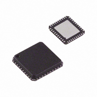
ADV7179KCPZ Analog Devices Inc, ADV7179KCPZ Datasheet - Page 34

ADV7179KCPZ
Manufacturer Part Number
ADV7179KCPZ
Description
IC ENCODER VID NTSC/PAL 40LFCSP
Manufacturer
Analog Devices Inc
Type
Video Encoderr
Datasheet
1.ADV7179KCPZ.pdf
(52 pages)
Specifications of ADV7179KCPZ
Applications
Digital Cameras, Mobile Phones, Portable Video
Voltage - Supply, Analog
2.8 V, 3.3 V
Mounting Type
Surface Mount
Package / Case
40-LFCSP
Input Format
Digital
Output Format
Analog
Supply Voltage Range
3V To 3.6V
Operating Temperature Range
0°C To +70°C
Tv / Video Case Style
LFCSP
No. Of Pins
40
Msl
MSL 1 - Unlimited
Lead Free Status / RoHS Status
Lead free / RoHS Compliant
Voltage - Supply, Digital
-
Lead Free Status / RoHS Status
Lead free / RoHS Compliant, Lead free / RoHS Compliant
Available stocks
Company
Part Number
Manufacturer
Quantity
Price
Company:
Part Number:
ADV7179KCPZ
Manufacturer:
ADI
Quantity:
250
Part Number:
ADV7179KCPZ
Manufacturer:
ADI/亚德诺
Quantity:
20 000
Company:
Part Number:
ADV7179KCPZ-REE1
Manufacturer:
SARC
Quantity:
92
Company:
Part Number:
ADV7179KCPZ-REEL
Manufacturer:
TI
Quantity:
69 456
Part Number:
ADV7179KCPZ-REEL
Manufacturer:
ADI/亚德诺
Quantity:
20 000
ADV7174/ADV7179
TIMING MODE REGISTER 1 (TR1)
Bits:
Address:
Timing Register 1 is an 8-bit-wide register. Figure 44 shows the various operations under the control of Timing Register 1. This register
can be read from as well written to. This register can be used to adjust the width and position of the master mode timing signals.
Table 16. TR1 Bit Description
Bit Name
HSYNC Width
HSYNC to FIELD/ VSYNC
Delay
HSYNC to FIELD Rising
Edge Delay
VSYNC Width
HSYNC to Pixel Data Adjust
TR17–TR10
SR4–SR0 = 08H
TR17 TR16
FIELD/VSYNC
TIMING MODE 1 (MASTER/PAL)
0
0
1
1
HSYNC TO PIXEL
DATA ADJUST
Bit No.
TR11–TR10
TR13–TR12
TR15–TR14
TR15–TR14
TR17–TR16
HSYNC
0
1
0
1
TR17
0 × T
1 × T
2 × T
3 × T
PCLK
PCLK
PCLK
PCLK
TR16
T
LINE 1
B
Description
These bits adjust the HSYNC pulse width.
These bits adjust the position of the HSYNC output relative to the FIELD/VSYNC output.
When the ADV7174/ADV7179 is in Timing Mode 1, these bits adjust the position of the HSYNC
output relative to the FIELD output rising edge.
When the ADV7174/ADV7179 is configured in Timing Mode 2, these bits adjust the VSYNC
pulse width.
This enables the HSYNC to be adjusted with respect to the pixel data. This allows the Cr and Cb
components to be swapped. This adjustment is available in both master and slave timing modes.
T
A
TR15 TR14
TR15 TR14
0
0
1
1
x
x
RISING EDGE DELAY
HSYNC TO FIELD
(MODE 1 ONLY)
(MODE 2 ONLY)
VSYNC WIDTH
TR15
0
1
0
1
0
1
1 × T
4 × T
16 × T
128 × T
Figure 44. Timing Register 1
T
T
B
B
Rev. B | Page 34 of 52
T
+ 32μs
TR14
PCLK
PCLK
C
PCLK
PCLK
TR13 TR12
0
0
1
1
TR13
FIELD/VSYNC DELAY
HSYNC TO
0
1
0
1
TR12
0 × T
4 × T
8 × T
16 × T
T
T
PCLK
PCLK
PCLK
C
B
PCLK
LINE 313
TR11
TR11 TR10
0
0
1
1
HSYNC WIDTH
0
1
0
1
LINE 314
TR10
1 × T
4 × T
16 × T
128 × T
T
PCLK
PCLK
A
PCLK
PCLK


