MC14490DWR2 ON Semiconductor, MC14490DWR2 Datasheet
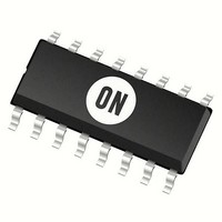
Arithmetic Logic Unit (ALU) LOG CMOS 3-18V HEX BOUNCE ELIMINATOR

MC14490DWR2

Manufacturer Part Number
MC14490DWR2
Description
Arithmetic Logic Unit (ALU) LOG CMOS 3-18V HEX BOUNCE ELIMINATOR
Manufacturer
ON Semiconductor
Datasheet

Specifications of MC14490DWR2

Package / Case
SOIC-16 Wide
Mounting Style
SMD/SMT
Number Of Circuits
Hex
Lead Free Status / Rohs Status
No

Available stocks

Company
Part Number
Manufacturer
Quantity
Price
Part Number:
MC14490DWR2G
Manufacturer:
ON
Quantity:
1 902
Part Number:
MC14490DWR2G
Manufacturer:
ON/安森美
Quantity:
20 000
MC14490
Hex Contact Bounce
Eliminator
enhancement mode devices, and is used for the elimination of
extraneous level changes that result when interfacing with mechanical
contacts. The digital contact bounce eliminator circuit takes an input
signal from a bouncing contact and generates a clean digital signal
four clock periods after the input has stabilized. The bounce eliminator
circuit will remove bounce on both the “make” and the “break” of a
contact closure. The clock for operation of the MC14490 is derived
from an internal R–C oscillator which requires only an external
capacitor to adjust for the desired operating frequency (bounce delay).
The clock may also be driven from an external clock source or the
oscillator of another MC14490 (see Figure 5).
are in indeterminate states.
2. Maximum Ratings are those values beyond which damage to the device
3. Temperature Derating:
MAXIMUM RATINGS
May, 2000 – Rev. 4
Symbol
V
The MC14490 is constructed with complementary MOS
NOTE: Immediately after power–up, the outputs of the MC14490
Line
Signal
Diode Protection on All Inputs
Six Debouncers Per Package
Internal Pullups on All Data Inputs
Can Be Used as a Digital Integrator, System Synchronizer, or Delay
Internal Oscillator (R–C), or External Clock Source
TTL Compatible Data Inputs/Outputs
Single Line Input, Debounces Both “Make” and “Break” Contacts
Does Not Require “Form C” (Single Pole Double Throw) Input
Cascadable for Longer Time Delays
Schmitt Trigger on Clock Input (Pin 7)
Supply Voltage Range = 3.0 V to 18 V
Chip Complexity: 546 FETs or 136.5 Equivalent Gates
in
Semiconductor Components Industries, LLC, 2000
may occur.
Plastic “P and D/DW” Packages: – 7.0 mW/ _ C From 65 _ C To 125 _ C
V
T
P
, V
T
T
I
stg
DD
in
D
A
L
out
DC Supply Voltage Range
Input or Output Voltage Range
Input Current
Power Dissipation,
Ambient Temperature Range
Storage Temperature Range
Lead Temperature
(DC or Transient)
(DC or Transient) per Pin
per Package (Note 3.)
(8–Second Soldering)
Parameter
(Voltages Referenced to V
– 0.5 to V
– 0.5 to +18.0
SS
– 55 to +125
– 65 to +150
) (Note 2.)
Value
500
260
10
DD
+ 0.5
1
Unit
mW
mA
V
V
C
C
C
against damage due to high static voltages or electric
fields. However, precautions must be taken to avoid ap-
plications of any voltage higher than maximum rated
voltages to this high–impedance circuit. For proper
operation, V
range V
logic voltage level (e.g., either V
puts must be left open.
1. For ordering information on the EIAJ version of
MC14490DW
MC14490DWR2
MC14490F
MC14490FEL
MC14490P
This device contains protection circuitry to guard
Unused inputs must always be tied to an appropriate
the SOIC packages, please contact your local
ON Semiconductor representative.
Device
SS
ORDERING INFORMATION
v
A
WL or L = Wafer Lot
YY or Y = Year
WW or W = Work Week
in
(V
and V
http://onsemi.com
in
or V
DW SUFFIX
CASE 751G
SOEIAJ–16
CASE 648
CASE 966
P SUFFIX
F SUFFIX
out
SOIC–16
SOEIAJ–16
SOEIAJ–16
PDIP–16
= Assembly Location
out
Package
SOIC–16
SOIC–16
PDIP–16
should be constrained to the
)
v
Publication Order Number:
V
DD
SS
.
or V
16
1000/Tape & Reel
1
16
16
1
1
DIAGRAMS
DD
See Note 1.
MARKING
See Note 1.
AWLYYWW
MC14490P
AWLYYWW
AWLYWW
Shipping
MC14490
). Unused out-
47/Rail
25/Rail
14490
MC14490/D

Related parts for MC14490DWR2

MC14490DWR2 Summary of contents

Page 1

... Maximum Ratings are those values beyond which damage to the device may occur. 3. Temperature Derating: Plastic “P and D/DW” Packages: – 7.0 mW From 125 _ C Semiconductor Components Industries, LLC, 2000 May, 2000 – Rev. 4 Device MC14490DW ) (Note 2.) SS Value Unit MC14490DWR2 – 0.5 to +18.0 V MC14490F – MC14490FEL MC14490P ...

Page 2

OSCILLATOR OSC 7 1 AND in TWO–PHASE CLOCK GENERATOR OSC 9 2 out B 14 IDENTICAL TO ABOVE STAGE IDENTICAL TO ABOVE STAGE IDENTICAL TO ABOVE STAGE in E ...

Page 3

ELECTRICAL CHARACTERISTICS Î Î Î Î Î ...

Page 4

SWITCHING CHARACTERISTICS Î Î Î Î Î Î Î Î Î Î Î Î Î Î Î Î Characteristic Î Î Î Î Î Î Î Î Î Î Î Î Î Î Î Î Î Î Î Î ...

Page 5

The MC14490 Hex Contact Bounce Eliminator is basically a digital integrator. The circuit can integrate both up and down. This enables the circuit to eliminate bounce on both the leading and trailing edges of the signal, shown in the timing ...

Page 6

DD PULLUP RESISTOR (INTERNAL “FORM A” CONTACT 7 OSC OSCILLATOR in AND C ext 9 TWO–PHASE CLOCK GENERATOR OSC out Figure 4. Typical “Form A” Contact Debounce Circuit The single most important characteristic of the MC14490 ...

Page 7

ASYMMETRICAL TIMING In applications where different leading and trailing edge delays are required (such as a fast attack/slow release timer.) Clocks of different frequencies can be gated into the MC14490 as shown in Figure 6. In order to produce a ...

Page 8

ACTIVE LOW B ACTIVE LOW Figure 9. Single Pulse Output Circuit OSC OR in OSC out INPUT Figure 10. Multiple Output Signal Timing Diagram MC14490 OUT BE 1 ...

Page 9

PACKAGE DIMENSIONS PLASTIC DIP PACKAGE –A– SEATING –T– PLANE 0.25 (0.010 MC14490 PDIP–16 P SUFFIX NOTES: CASE 648–08 1. DIMENSIONING AND TOLERANCING PER ...

Page 10

PLASTIC EIAJ SOIC PACKAGE VIEW 0.10 (0.004) 0.13 (0.005) M MC14490 PACKAGE DIMENSIONS SOEIAJ–16 F SUFFIX CASE 966–01 ISSUE O NOTES ...

Page 11

PACKAGE DIMENSIONS PLASTIC SOIC PACKAGE 16X 0. SEATING e PLANE 14X T MC14490 SOIC–16 DW SUFFIX CASE 751G–03 ISSUE B q NOTES: 1. DIMENSIONS ARE IN ...

Page 12

... CENTRAL/SOUTH AMERICA: Spanish Phone: 303–308–7143 (Mon–Fri 8:00am to 5:00pm MST) Email: ONlit–spanish@hibbertco.com ASIA/PACIFIC: LDC for ON Semiconductor – Asia Support Phone: 303–675–2121 (Tue–Fri 9:00am to 1:00pm, Hong Kong Time) Toll Free from Hong Kong & Singapore: 001–800–4422–3781 Email: ONlit– ...

Related keywords