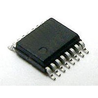
Si8442BA-D-IU Silicon Laboratories Inc, Si8442BA-D-IU Datasheet - Page 25

Si8442BA-D-IU
Manufacturer Part Number
Si8442BA-D-IU
Description
Isolator Interface IC Quad Ch 1 kV Iso 150M 2/2
Manufacturer
Silicon Laboratories Inc
Specifications of Si8442BA-D-IU
Number Of Channels
4
Propagation Delay Time
35 ns
Supply Voltage (max)
5.5 V
Supply Voltage (min)
2.7 V
Supply Current
9 mA
Power Dissipation
275 mW
Maximum Operating Temperature
+ 125 C
Mounting Style
SMD/SMT
Package / Case
QSOP-16
Minimum Operating Temperature
- 40 C
Lead Free Status / Rohs Status
Details
3. Errata and Design Migration Guidelines
The following errata apply to Revision C devices only. See "5. Ordering Guide" on page 27 for more details. No
errata exist for Revision D devices.
3.1. Enable Pin Causes Outputs to Go Low (Revision C Only)
When using the enable pin (EN1, EN2) function on the 4-channel (Si8440/1/2) isolators, the corresponding output
pin states (pin = An, Bn, where n can be 1…4) are driven to a logic low (to ground) when the enable pin is disabled
(EN1 or EN2 = 0). This functionality is different from the legacy 4-channel (Si8440/1/2) isolators. On those devices,
the isolator outputs go into a high-impedance state (Hi-Z) when the enable pin is disabled (EN1 = 0 or EN2 = 0).
3.1.1. Resolution
The enable pin functionality causing the outputs to go low is supported in production for Revision C of the Si844x
devices. Revision D corrects the enable pin functionality (i.e., the outputs will go into the high-impedance state to
match the legacy isolator products). Refer to the Ordering Guide sections of the data sheet(s) for current ordering
information.
3.2. Power Supply Bypass Capacitors (Revision C and Revision D)
When using the Si844x isolators with power supplies > 4.5 V, sufficient VDD bypass capacitors must be present on
both the VDD1 and VDD2 pins to ensure the VDD rise time is less than 0.5 V/µs (which is > 9 µs for a > 4.5 V
supply). Although rise time is power supply dependent, > 1 µF capacitors are required on both power supply pins
(VDD1, VDD2) of the isolator device.
3.2.1. Resolution
For recommendations on resolving this issue, see "2.4.1. Supply Bypass" on page 22. Additionally, refer to "5.
Ordering Guide" on page 27 for current ordering information.
3.3. Latch Up Immunity (Revision C Only)
Latch up immunity generally exceeds ± 200 mA per pin. Exceptions: Certain pins provide < 100 mA of latch-up
immunity. To increase latch-up immunity on these pins, 100 of equivalent resistance must be included in series
with all of the pins listed in Table 14. The 100 equivalent resistance can be comprised of the source driver's
output resistance and a series termination resistor. The Si8441 is not affected when using power supply voltages
(VDD1 and VDD2) < 3.5 V.
3.3.1. Resolution
This issue has been corrected with Revision D of the device. Refer to “5. Ordering Guide” for current ordering
information.
Affected Ordering Part Numbers*
SI8440SV-C-IS/IS1, SI8441SV-C-IS/IS1,
SI8442SV-C-IS/IS1
SI8445SV-C-IS/IS1
*Note: SV = Speed Grade/Isolation Rating (AA, AB, BA, BB).
Table 14. Affected Ordering Part Numbers (Revision C Only)
Revision
Device
C
C
Rev. 1.4
Pin#
10
14
14
6
6
Si8440/41/42/45
Name
EN2
A4
B1
A4
B1
Input or Output
Pin Type
Output
Output
Input
Input
25


