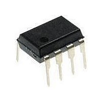
ATTINY12V-1PU Atmel, ATTINY12V-1PU Datasheet - Page 57

ATTINY12V-1PU
Manufacturer Part Number
ATTINY12V-1PU
Description
Microcontrollers (MCU) AVR 1K FLASH 64B EE 1.8V 1MHZ
Manufacturer
Atmel
Datasheet
1.ATTINY12V-1SI.pdf
(94 pages)
Specifications of ATTINY12V-1PU
Processor Series
ATTINY1x
Core
AVR8
Data Bus Width
8 bit
Program Memory Type
Flash
Program Memory Size
1 KB
Maximum Clock Frequency
1.2 MHz
Number Of Programmable I/os
6
Number Of Timers
1
Maximum Operating Temperature
+ 85 C
Mounting Style
Through Hole
Package / Case
PDIP-8
3rd Party Development Tools
EWAVR, EWAVR-BL
Minimum Operating Temperature
- 40 C
Package
8PDIP
Device Core
AVR
Family Name
ATtiny
Maximum Speed
1.2 MHz
Operating Supply Voltage
2.5|3.3|5 V
Interface Type
SPI
Operating Temperature
-40 to 85 °C
Lead Free Status / Rohs Status
Details
Table 25. Low-voltage Serial Programming Instruction Set
Note:
Note:
1006F–AVR–06/07
Instruction
Programming Enable
Chip Erase
Read Program Memory
Write Program Memory
Read EEPROM
Memory
Write EEPROM
Memory
Write Lock Bits
Read Lock Bits
Read Signature Bytes
Read Calibration Byte
Write Fuse Bits
Read Fuse Bits
a = address high bits
b = address low bits
H = 0 - Low byte, 1 - High byte
o = data out
i = data in
x = don’t care
1 = Lock bit 1
2 = Lock bit 2
3 = CKSEL0 Fuse
4 = CKSEL1 Fuse
5 = CKSEL2 Fuse
6 = CKSEL3 Fuse
7 = RSTDISBL Fuse
8 = SPIEN Fuse
9 = BODEN Fuse
A = BODLEVEL Fuse
1. The signature bytes are not readable in Lock mode 3, i.e. both lock bits programmed.
1010 1100
1010 1100
0010 H000
0100 H000
1010 0000
1100 0000
1010 1100
0101 1000
0011 0000
0011 1000
1010 1100
0101 0000
Byte 1
0101 0011
100x xxxx
xxxx xxxa
xxxx xxxa
xxxx xxxx
xxxx xxxx
1111 1211
xxxx xxxx
xxxx xxxx
xxxx xxxx
101x xxxx
xxxx xxxx
Byte 2
Instruction Format
xxxx xxxx
xxxx xxxx
bbbb bbbb
bbbb bbbb
xxbb bbbb
xxbb bbbb
xxxx xxxx
xxxx xxxx
0000 00bb
0000 0000
xxxx xxxx
xxxx xxxx
Byte 3
xxxx xxxx
xxxx xxxx
oooo oooo
iiii iiii
oooo oooo
iiii iiii
xxxx xxxx
xxxx x21x
oooo oooo
oooo oooo
A987 6543
A987 6543
Byte4
Operation
Enable serial programming while
RESET is low.
Chip erase Flash and EEPROM
memory arrays.
Read H (high or low) data o from
program memory at word address
a:b.
Write H (high or low) data i to
program memory at word address
a:b.
Read data o from EEPROM memory
at address b.
Write data i to EEPROM memory at
address b.
Write lock bits. Set bits 1,2 = “0” to
program lock bits.
Read lock bits. “0” = programmed, “1”
= unprogrammed.
Read signature byte o at address b.
Set bits A, 9 - 3 = “0” to program, “1”
to unprogram.
Read fuse bits. “0” = programmed, “1”
= unprogrammed.
ATtiny11/12
(1)
57


