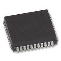
VRS51C1000-40-LG Ramtron, VRS51C1000-40-LG Datasheet - Page 22

VRS51C1000-40-LG
Manufacturer Part Number
VRS51C1000-40-LG
Description
Microcontrollers (MCU) 64K+1K 40MHz 5V
Manufacturer
Ramtron
Datasheet
1.VRS51C1000-40-PG.pdf
(48 pages)
Specifications of VRS51C1000-40-LG
Data Bus Width
8 bit
Program Memory Type
Flash
Program Memory Size
64 KB
Data Ram Size
1 KB
Interface Type
UART
Maximum Clock Frequency
40 MHz
Number Of Programmable I/os
36
Number Of Timers
3
Operating Supply Voltage
4.5 V to 5.5 V
Maximum Operating Temperature
+ 85 C
Mounting Style
SMD/SMT
Package / Case
PLCC-44
Minimum Operating Temperature
- 40 C
Lead Free Status / Rohs Status
Details
T
UART Operating Modes
The VRS51C1000’s serial port can operate in four
different Modes. In all four Modes, a transmission is
initiated by an instruction that uses the SBUF register
as a destination register. In Mode 0, reception is
initiated by setting RI to 0 and REN to 1. An incoming
start bit initiates reception in the other modes, provided
that REN is set to 1. The following paragraphs
describe these four Modes.
UART Operation in Mode 0
In this Mode, the serial data exits and enters through
the RXD pin. TXD is used to output the shift clock. The
signal is composed of 8 data bits starting with the LSB.
The baud rate in this mode is 1/12 the oscillator
frequency.
______________________________________________________________________________________________
www.ramtron.com
F
ABLE
IGURE
SM0
0
0
1
1
Write to
VRS51C1000
SBUF
REN
Fosc/12
RI
31: S
16: S
Input Function
ERIAL
SM1
0
1
0
1
ERIAL
1
RXD P3.0
P
D
S
CLK
ORT
P
Start
TX Clock
RX Clock
Start Shift
ORT
Q
M
Mode
0
1
2
3
M
ODES OF
ODE
ZERO DETECTOR
RX Control Unit
1
TX Control Unit
1
0 B
Internal Bus
Shift Register
TI
RI
1
Internal Bus
O
LOCK
SBUF
SBUF
1
PERATION
Description
Shift Register
8-bit UART
9-bit UART
9-bit UART
1
Shift
1
D
Receive
IAGRAM
1
Serial Port
Interrupt
0
Send
Shift
READ SBUF
RXD P3.0
Clock
Shift
RXD P3.0
Baud Rate
F
Variable
F
F
Variable
TXD P3.1
osc
osc
osc
/12
/64
/32
or
UART Transmission in Mode 0
Any instruction that uses SBUF as a destination
register may initiate a transmission. The “write to
SBUF” signal also loads a 1 into the 9
transmit shift register and informs the TX control block
to begin a transmission. The internal timing is such that
one full machine cycle will elapse between a write to
SBUF instruction and the activation of SEND.
The SEND signal enables the output of the shift
register to the alternate output function line of P3.0 and
enables SHIFT CLOCK to the alternate output function
line of P3.1.
At every machine cycle in which SEND is active, the
contents of the transmit shift register are shifted to the
right by one position.
Zeros come in from the left as data bits shift out to the
right. The TX control block sends its final shift and de-
activates SEND while setting T1 after one condition is
fulfilled.
output position of the shift register; the 1 that was
initially loaded into the 9
the MSB; and all positions to the left of that contain
zeros. Once these conditions are met, the de-
activation of SEND and the setting of T1 occurs at T1
of the 10
pulse.
UART Reception in Mode 0
When REN and R1 are set to 1 and 0, respectively,
reception is initiated. The bits 11111110 are written to
the receive shift register at the end of the next machine
cycle by the RX control unit. In the following phase, the
RX control unit will activate RECEIVE.
The contents of the receive shift register are shifted
one position to the left at the end of every machine
cycle during which RECEIVE is active. The value that
comes in from the right is the value that was sampled
at the P3.0 pin.
1’s are shifted out to the left as data bits are shifted in
from the right. The RX control block is flagged to do
one last shift and load SBUF when the 0 that was
initially loaded into the rightmost position arrives at the
leftmost position in the shift register.
th
When the MSB of the data byte is at the
machine cycle after the “write to SBUF”
th
position is just to the left of
page 22 of 48
th
position of the


