VRS51C1000-40-LG-ISPV2 Ramtron, VRS51C1000-40-LG-ISPV2 Datasheet - Page 3
VRS51C1000-40-LG-ISPV2
Manufacturer Part Number
VRS51C1000-40-LG-ISPV2
Description
Microcontrollers (MCU) 64K+1K 40MHz 5V
Manufacturer
Ramtron
Datasheet
1.VRS51C1000-40-PG.pdf
(48 pages)
Specifications of VRS51C1000-40-LG-ISPV2
Data Bus Width
8 bit
Program Memory Type
Flash
Program Memory Size
64 KB
Data Ram Size
1 KB
Interface Type
UART
Maximum Clock Frequency
40 MHz
Number Of Programmable I/os
36
Number Of Timers
3
Operating Supply Voltage
4.5 V to 5.5 V
Maximum Operating Temperature
+ 85 C
Mounting Style
SMD/SMT
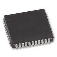
Package / Case
PLCC-44
Minimum Operating Temperature
- 40 C
Lead Free Status / Rohs Status
Details


VRS51C1000 DIP-40 Pin Descriptions
T
______________________________________________________________________________________________
www.ramtron.com
ABLE
VRS51C1000
DIP40
10
11
12
13
14
15
16
17
18
19
20
1
2
3
4
5
6
7
8
9
2: VRS51C1000 P
PWM0 / P1.3
PWM1 / P1.4
PWM2 / P1.5
PWM3 / P1.6
PWM4 / P1.7
#INT0 / P3.2
#INT1 / P3.3
T2EX / P1.1
T2
P1.0
T2EX
P1.1
P1.2
PWM0
P1.3
PWM1
P1.4
PWM2
P1.5
PWM3
P1.6
PWM4
P1.7
RESET
RXD
P3.0
TXD
P3.1
#INT0
P3.2
#INT1
P3.3
T0
P3.4
T1
P3.5
#WR
P3.6
#RD
P3.7
XTAL2
XTAL1
VSS
#WR / P3.6
RXD / P3.0
TXD / P3.1
#RD / P3.7
Name
T2 / P1.0
T0 / P3.4
T1 / P3.5
RESET
XTAL2
XTAL1
P1.2
VSS
IN
D
I
I/O
I
I/O
I/O
O
I/O
O
I/O
O
I/O
O
I/O
O
I/O
I
I
I/O
O
I/O
I
I/O
I
I/O
I
I/O
I
I/O
O
I/O
O
I/O
O
I
-
ESCRIPTIONS FOR
I/O
1
2
3
4
5
6
7
8
9
10
11
12
13
14
15
16
17
18
19
20
VRS51C1000
Timer 2 Clock Out
Bit 0 of Port 1
Timer 2 Control
Bit 1 of Port 1
Bit 2 of Port 1
PWM Channel 0
Bit 3 of Port 1
PWM Channel 1
Bit 4 of Port 1
PWM Channel 2
Bit 5 of Port 1
PWM Channel 3
Bit 6 of Port 1
PWM Channel 4
Bit 7 of Port 1
Reset
Receive Data
Bit 0 of Port 3
Transmit Data &
Bit 1 of Port 3
External Interrupt 0
Bit 2 of Port 3
External Interrupt 1
Bit 3 of Port 3
Timer 0
Bit 4 of Port 3
Timer 1 & 3
Bit 5 of Port
Ext. Memory Write
Bit 6 of Port 3
Ext. Memory Read
Bit 7 of Port 3
Oscillator/Crystal Output
Oscillator/Crystal In
Ground
DIP-40
DIP40
Function
40
39
38
37
36
35
34
33
32
31
30
29
28
27
26
25
24
23
22
21
PACKAGE
VDD
P0.0 / AD0
P0.1 / AD1
P0.2 / AD2
P0.3 / AD3
P0.4 / AD4
P0.5 / AD5
P0.6 / AD6
P0.7 / AD7
#EA / VPP
ALE
PSEN
P2.7 / A15
P2.6 / A14
P2.5 / A13
P2.4 / A12
P2.3 / A11
P2.2 / A10
P2.1 / A9
P2.0 / A8
DIP40
21
22
23
24
25
26
27
28
29
30
31
32
33
34
35
36
37
38
39
40
P2.0
A8
P2.1
A9
P2.2
A10
P2.3
A11
P2.4
A12
P2.5
A13
P2.6
A14
P2.7
A15
#PSEN
ALE
#EA /
VPP
P0.7
AD7
P0.6
AD6
P0.5
AD5
P0.4
AD4
P0.3
AD3
P0.2
AD2
P0. 1
AD1
P0.0
AD0
VDD
Name
I/O
O
I/O
O
I/O
O
I/O
O
I/O
O
I/O
O
I/O
O
I/O
O
O
O
I
I/O
I/O
I/O
I/O
I/O
I/O
I/O
I/O
I/O
I/O
I/O
I/O
I/O
I/O
I/O
I/O
-
I/O
Bit 0 of Port 2
Bit 8 of External Memory Address
Bit 1 of Port 2
Bit 9 of External Memory Address
Bit 2 of Port 2
Bit 10 of External Memory Address
Bit 3 of Port 2 &
Bit 11 of External Memory Address
Bit 4 of Port 2
Bit 12 of External Memory Address
Bit 5 of Port 2
Bit 13 of External Memory Address
Bit 6 of Port 2
Bit 14 of External Memory Address
Bit 7 of Port 2
Bit 15 of External Memory Address
Program Store Enable
Address Latch Enable
External Access
Flash programming voltage input
Bit 7 Of Port 0
Data/Address Bit 7 of External
Memory
Bit 6 of Port 0
Data/Address Bit 6 of External
Memory
Bit 5 of Port 0
Data/Address Bit 5 of External
Memory
Bit 4 of Port 0
Data/Address Bit 4 of External
Memory
Bit 3 Of Port 0
Data/Address Bit 3 of External
Memory
Bit 2 of Port 0
Data/Address Bit 2 of External
Memory
Bit 1 of Port 0 & Data
Address Bit 1 of External Memory
Bit 0 Of Port 0 & Data
Address Bit 0 of External Memory
Supply input
Function
page 3 of 48
Related parts for VRS51C1000-40-LG-ISPV2
Image
Part Number
Description
Manufacturer
Datasheet
Request
R

Part Number:
Description:
Microcontrollers (MCU) 64K+1K 40MHz 5V
Manufacturer:
Ramtron
Datasheet:

Part Number:
Description:
Microcontrollers (MCU) 64K+1K 40MHz 5V
Manufacturer:
Ramtron
Datasheet:

Part Number:
Description:
Microcontrollers (MCU) 64K+1K 40MHz 5V
Manufacturer:
Ramtron
Datasheet:
Part Number:
Description:
Microcontrollers (MCU) 64K+1K 40MHz 5V
Manufacturer:
Ramtron
Datasheet:

Part Number:
Description:
Versa 8051 MCU with 64KB of IAP/ISP Flash
Manufacturer:
RAMTRON [Ramtron International Corporation]
Datasheet:
Part Number:
Description:
Versa 8051 Mcu With 64kb Of Iap/isp Flash
Manufacturer:
Ramtron Corporation
Datasheet:
Part Number:
Description:
8-bit Microcontrollers - MCU 64K+1K 40MHz 5V
Manufacturer:
Cypress Semiconductor
Part Number:
Description:
8-bit Microcontrollers - MCU 64K+1K 40MHz 5V
Manufacturer:
Cypress Semiconductor
Part Number:
Description:
8-bit Microcontrollers - MCU 64K+1K 40MHz 5V
Manufacturer:
Cypress Semiconductor
Part Number:
Description:
8-bit Microcontrollers - MCU 64K+1K 40MHz 5V
Manufacturer:
Cypress Semiconductor
Part Number:
Description:
8-bit Microcontrollers - MCU 64K+1K 40MHz 5V
Manufacturer:
Cypress Semiconductor
Part Number:
Description:
8-bit Microcontrollers - MCU 64K+1K 40MHz 5V
Manufacturer:
Cypress Semiconductor

Part Number:
Description:
SOP28
Manufacturer:
Ramtron
Datasheet: