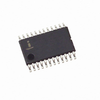
ISL83387EIV-T Intersil, ISL83387EIV-T Datasheet - Page 6

ISL83387EIV-T
Manufacturer Part Number
ISL83387EIV-T
Description
IC 3DRVR/3RCVR RS232 3V 24-TSSOP
Manufacturer
Intersil
Type
Transceiverr
Datasheet
1.ISL83387EIVZ.pdf
(13 pages)
Specifications of ISL83387EIV-T
Number Of Drivers/receivers
3/3
Protocol
RS232
Voltage - Supply
3 V ~ 5.5 V
Mounting Type
Surface Mount
Package / Case
24-TSSOP
Lead Free Status / RoHS Status
Contains lead / RoHS non-compliant
Detailed Description
The ISL83387E operates from a single +3V to +5.5V supply,
guarantees a 250kbps minimum data rate, requires only four
small external 0.1µF capacitors, features low power
consumption, and meets all ElA RS-232C and V.28
specifications. The circuit is divided into three sections: The
charge pump, the transmitters, and the receivers.
Charge-Pump
Intersil’s new ISL83387E utilizes regulated on-chip dual
charge pumps as voltage doublers, and voltage inverters to
generate ±5.5V transmitter supplies from a V
low as 3.0V. This allows these devices to maintain RS-232
compliant output levels over the ±10% tolerance range of
3.3V powered systems. The efficient on-chip power supplies
require only four small, external 0.1µF capacitors for the
voltage doubler and inverter functions over the full V
range; other capacitor combinations can be used as shown
in Table 3. The charge pumps operate discontinuously (i.e.,
they turn off as soon as the V+ and V- supplies are pumped
up to the nominal values), resulting in significant power
savings.
Transmitters
The transmitters are proprietary, low dropout, inverting
drivers that translate TTL/CMOS inputs to EIA/TIA-232
output levels. Coupled with the on-chip ±5.5V supplies,
these transmitters deliver true RS-232 levels over a wide
range of single supply system voltages.
All transmitter outputs disable and assume a high
impedance state when the device enters the powerdown
mode (see Table 2). These outputs may be driven to ±12V
when disabled.
All devices guarantee a 250kbps data rate for full load
conditions (3kΩ and 1000pF), V
transmitter operating at full speed. Under more typical
conditions of V
transmitter easily operates at 1.25Mbps.
The transmitter input threshold is set by the voltage applied
to the V
unconnected (there are no pull-up resistors), and may cause
I
performance.
Receivers
The ISL83387E contains standard inverting receivers that
convert RS-232 signals to CMOS output levels and accept
inputs up to ±25V while presenting the required 3kΩ to 7kΩ
input impedance (see Figure 1) even if the power is off
(V
hysteresis to increase noise immunity and decrease errors
due to slow input signal transitions. Receiver outputs swing
CC
CC
increases. Connect unused inputs to GND for the best
= 0V). The receivers’ Schmitt trigger input stage uses
L
supply pin. Transmitter inputs float if left
CC
≥ 3.3V, R
L
= 3kΩ, and C
6
CC
≥ 3.0V, with one
L
= 250pF, one
CC
supply as
CC
ISL83387E
from GND to V
Table 2).
Low Power Operation
This 3V device requires a nominal supply current of 0.3mA,
even at V
powerdown mode). This is considerably less than the 11mA
current required by comparable 5V RS-232 devices, allowing
users to reduce system power simply by replacing the old
style device with the ISL83387E in new designs.
Powerdown Functionality
The already low current requirement drops significantly
when the device enters powerdown mode. In powerdown,
supply current drops to 1µA, because the on-chip charge
pump turns off (V+ collapses to V
and the transmitter outputs tristate. This micro-power mode
makes these devices ideal for battery powered and portable
applications.
Software Controlled (Manual) Powerdown
This device allows the user to force the IC into the low
power, standby state, and utilizes a two pin approach where
the FORCEON and FORCEOFF inputs determine the IC’s
mode. For always enabled operation, FORCEON and
FORCEOFF are both strapped high. To switch between
active and powerdown modes, under logic or software
control, only the FORCEOFF input need be driven. The
FORCEON state isn’t critical, as FORCEOFF dominates
over FORCEON. Nevertheless, if strictly manual control over
powerdown is desired, the user must strap FORCEON high
to disable the enhanced automatic powerdown circuitry.
Connecting FORCEOFF and FORCEON together disables
the enhanced automatic powerdown feature, enabling them
to function as a manual SHUTDOWN input (see Figure 2).
With any of the above control schemes, the time required to
exit powerdown, and resume transmission is only 100µs.
When using both manual and enhanced automatic
powerdown (FORCEON = 0), the ISL83387E won’t power
up from manual powerdown until both FORCEOFF and
FORCEON are driven high, or until a transition occurs on a
receiver or transmitter input. Figure 3 illustrates a circuit for
ensuring that the ISL83387E powers up as soon as
FORCEOFF switches high. The rising edge of the Master
Powerdown signal forces the device to power up, and the
ISL83387E returns to enhanced automatic powerdown
-25V ≤ V
CC
FIGURE 1. RECEIVER CONNECTIONS
= 5.5V, during normal operation (not in
RIN
R
GND
L
, and do not tristate in powerdown (see
XIN
V
≤ +25V
L
5kΩ
CC
, V- collapses to GND),
GND ≤ V
R
XOUT
ROUT
≤ V
July 8, 2005
L
FN6040.1


