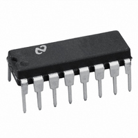
DS8832N National Semiconductor, DS8832N Datasheet - Page 4

DS8832N
Manufacturer Part Number
DS8832N
Description
IC DRIVER DUAL TRISTATE 16-DIP
Manufacturer
National Semiconductor
Type
Driverr
Datasheet
1.DS8832N.pdf
(11 pages)
Specifications of DS8832N
Number Of Drivers/receivers
4/0
Voltage - Supply
4.75 V ~ 5.25 V
Mounting Type
Through Hole
Package / Case
16-DIP (0.300", 7.62mm)
Lead Free Status / RoHS Status
Contains lead / RoHS non-compliant
Protocol
-
Other names
*DS8832N
Available stocks
Company
Part Number
Manufacturer
Quantity
Price
www.national.com
t
t
H1
H0
Symbol
T
Switching Characteristics
Note 2: “Absolute Maximum Ratings” are those values beyond which the safety of the device cannot be guaranteed. Except for “Operating Temperature Range” they
are not meant to imply that the devices should be operated at these limits. The table of “Electrical Characteristics” provides conditions for actual device operation.
Note 3: Unless otherwise specified min/max limits apply across the −55˚C to +125˚C temperature range for the DS7831 and across the 0˚C to +70˚C range for the
DS8832. All typical values are for T
Note 4: All currents into device pins shown as positive, out of device pins as negative, all voltage referenced to ground unless otherwise noted. All values shown
as max or min on absolute value basis.
Note 5: Applies for T
Mode of Operation
To operate as a quad single-ended line driver apply logical
“0”s to the output disable pins (to keep the outputs in the nor-
mal low impedance mode) and apply logical “0”s to both
Differential/Single-ended Mode Control inputs. All four chan-
nels will then operate independently and no signal inversion
will occur between inputs and outputs.
To operate as a dual differential line driver apply logical “0”s
to the Output Disable pins and apply at least one logical “1”
to the Differential/Single-ended Mode Control inputs.
The inputs to the A channels should be connected together
and the inputs to the B channels should be connected to-
gether.
In this mode the signals applied to the resulting inputs will
pass non-inverted on the A
the A
When operating in a bus-organized system with outputs tied
directly to outputs of other DS7831, DS8832’s ( Figure 1 ), all
devices except one must be placed in the “high impedance”
A
= 25˚C, V
1
and B
Propagation Delay from Disable Inputs
to Logical “1” Level (from High
Impedance State)
Propagation Delay from Disable Inputs
to Logical “0” Level (from High
Impedance State)
CC
1
outputs.
= 5V, unless otherwise noted
A
= 125˚C only. Only one output should be shorted at a time.
2
Parameter
A
and B
= 25˚C and V
2
outputs and inverted on
CC
= 5V.
(Continued)
FIGURE 1.
4
state. This is accomplished by ensuring that a logical “1” is
applied to at least one of the Output Disable pins of each de-
vice which is to be in the “high impedance” state. A NOR gate
was purposely chosen for this function since it is possible
with only two DM5442/DM7442, BCD-to-decimal decoders,
to decode as many as 100 DS7831, DS8832’s ( Figure 2 ).
The unique device whose Disable inputs receive two logical
“0” levels assumes the normal low impedance output state,
providing good capacitive drive capability and waveform in-
tegrity especially during the transition from the logical “0” to
logical ”1” state. The other outputs — in the high impedance
state — take only a small amount of leakage current from the
low impedance outputs. Since the logical “1” output current
from the selected device is 100 times that of a conventional
Series 54/74 device (40 mA vs. 400 µA), the output is easily
able to supply that leakage current for several hundred other
DS7831/DS8831’s, DS7832/DS8832’s and still have avail-
able drive for the bus line ( Figure 3 ).
Conditions
DS005800-2
Min
Typ
14
18
Max
22
27
Units
ns
ns


