DS26F31CJ National Semiconductor, DS26F31CJ Datasheet - Page 2
DS26F31CJ
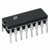
Manufacturer Part Number
DS26F31CJ
Description
IC LINE DRIVER QUAD HS 16-DIP
Manufacturer
National Semiconductor
Type
Line Driver, Transmitterr
Datasheet
1.DS26F31CJ.pdf
(6 pages)
Specifications of DS26F31CJ
Number Of Drivers/receivers
4/0
Protocol
RS422
Voltage - Supply
4.75 V ~ 5.25 V
Mounting Type
Through Hole
Package / Case
*
Lead Free Status / RoHS Status
Contains lead / RoHS non-compliant
Other names
*DS26F31CJ
Available stocks
Company
Part Number
Manufacturer
Quantity
Price


http
Symbol
V
V
V
V
I
I
I
I
V
I
I
I
t
t
SKEW
t
t
t
t
Absolute Maximum Ratings
If Military Aerospace specified devices are required
please contact the National Semiconductor Sales
Office Distributors for availability and specifications
Storage Temperature Range
Lead Temperature
Maximum Power Dissipation at 25 C
Supply Voltage
Input Voltage
Output Voltage
Electrical Characteristics
Note 1 ‘‘Absolute Maximum Ratings’’ are those values beyond which the safety of the device cannot be guaranteed They are not meant to imply that the devices
should be operated at these limits The tables of ‘‘Electrical Characteristics’’ provide conditions for actual device operation
Note 2 Unless otherwise specified min max limits apply across the
for the DS26F31C All typicals are given for V
Note 3 All currents into the device pins are positive all currents out of the device pins are negative All voltages are referenced to ground unless otherwise
specified
Note 4 Only one output at a time should be shorted
Note 5 C
Note 6 Skew is defined as the difference in propagation delays between complementary outputs at the 50% point
IL
IH
IR
OZ
OS
CCX
CC
PLH
PHL
LZ
HZ
ZL
ZH
Derate cavity package 10 mW C above 25 C
OH
OL
IH
IL
IC
www national com
Ceramic DIP
Ceramic DIP (Soldering 60 sec )
Cavity Package
L
e
30 pF V
Output Voltage HIGH
Output Voltage LOW
Input Voltage HIGH
Input Voltage LOW
Input Current LOW
Input Current HIGH
Input Reverse Current
Off State (High Impedance)
Output Current
Input Clamp Voltage
Output Short Circuit
Supply Current
Input to Output
Input to Output
Output to Output
Enable to Output
Enable to Output
Enable to Output
Enable to Output
I
e
Parameter
1 3V to V
O
e
1 3V V
CC
e
PULSE
b
5V and T
over operating range unless otherwise specified (Notes 2
65 C to
e
V
V
V
V
V
V
V
V
V
V
V
V
V
Load
V
Load
V
Load
V
C
V
C
V
Load
V
Load
0V to
(Note 1)
CC
CC
CC
CC
CC
CC
CC
CC
CC
CC
CC
CC
CC
CC
CC
CC
CC
CC
CC
L
L
A
e
e
1500 mW
e
a
e
e
e
e
e
e
e
e
e
e
e
e
e
e
e
e
e
e
e
a
e
e
e
e
e
10 pF
10 pF
25 C
b
175 C
300 C
3V (See AC Load Test Circuit for TRI-STATE Outputs)
Min I
Min I
Min
Max
Max V
Max V
Max V
Max
Min I
Max (Note 4)
Max All Outputs Disabled
Max All Outputs Enabled
5 0V T
5 0V T
5 0V T
5 0V T
5 0V T
5 0V T
5 0V T
7 0V
7 0V
5 5V
Note 5 Note 6
Note 5
Note 5 Note 6
Note 5
Note 5
55 C to
Conditions
OH
OL
I
e b
I
I
I
A
A
A
A
A
A
A
a
e
e
e
e
2
e b
e
e
e
e
e
e
e
125 C temperature range for the DS26F31M and across the O C to
0 4V
2 7V
7 0V
20 mA
18 mA
25 C
25 C
25 C
25 C
25 C
25 C
25 C
V
V
Operating Range
DS26F31C
DS26F31M
20 mA
O
O
Temperature
Supply Voltage
Temperature
Supply Voltage
e
e
2 5V
0 5V
b
Min
2 5
2 0
30
b
0 001
b
0 32
b
Typ
3 2
0 5
0 5
0 5
2 0
10
10
23
15
20
23
0 10
0 8
60
3)
b
b
b
b
b
Max
55 C to
0 5
0 8
0 1
4 5
20
20
50
40
15
15
32
25
30
32
0 20
150
1 5
4 75V to 5 25V
20
0 C to
4 5V to 5 5V
a
70 C range
a
a
125 C
Units
70 C
mA
mA
mA
mA
mA
ns
ns
ns
ns
ns
ns
ns
V
V
V
V
V
A
A
Related parts for DS26F31CJ
Image
Part Number
Description
Manufacturer
Datasheet
Request
R

Part Number:
Description:
National Semiconductor [8-Bit D/A Converter]
Manufacturer:
National Semiconductor
Datasheet:
Part Number:
Description:
National Semiconductor [Media Coprocessor]
Manufacturer:
National Semiconductor
Datasheet:
Part Number:
Description:
Digitally Controlled Tone and Volume Circuit with Stereo Audio Power Amplifier, Microphone Preamp Stage and National 3D Sound
Manufacturer:
National Semiconductor
Datasheet:
Part Number:
Description:
Digitally Controlled Tone and Volume Circuit with Stereo Audio Power Amplifier, Microphone Preamp Stage and National 3D Sound
Manufacturer:
National Semiconductor
Datasheet:
Part Number:
Description:
AC97 Rev 2 Codec with Sample Rate Conversion and National 3D Sound
Manufacturer:
National Semiconductor
Part Number:
Description:
Manufacturer:
National Semiconductor
Datasheet:
Part Number:
Description:
Manufacturer:
National Semiconductor
Datasheet:
Part Number:
Description:
General Purpose, Low Voltage, Low Power, Rail-to-Rail Output Operational Amplifiers
Manufacturer:
National Semiconductor
Datasheet:
Part Number:
Description:
8-bit 20 MSPS flash A/D converter.
Manufacturer:
National Semiconductor
Datasheet:
Part Number:
Description:
Low Noise Quad Operational Amplifier
Manufacturer:
National Semiconductor
Datasheet:
Part Number:
Description:
Quad Differential Line Receivers
Manufacturer:
National Semiconductor
Datasheet:
Part Number:
Description:
Quad High Speed Trapezoidal? Bus Transceiver
Manufacturer:
National Semiconductor
Datasheet:
Part Number:
Description:
Dual Line Receiver
Manufacturer:
National Semiconductor
Datasheet:
Part Number:
Description:
TTL to 10k ECL Level Translator with Latch
Manufacturer:
National Semiconductor
Datasheet: