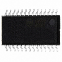
ST7540 STMicroelectronics, ST7540 Datasheet - Page 21

ST7540
Manufacturer Part Number
ST7540
Description
IC TXRX FSK POWER LINE 28-TSSOP
Manufacturer
STMicroelectronics
Type
Transceiverr
Datasheet
1.ST7540TR.pdf
(44 pages)
Specifications of ST7540
Number Of Drivers/receivers
1/1
Voltage - Supply
5 V ~ 9 V
Mounting Type
Surface Mount
Package / Case
28-TSSOP Exposed Pad, 28-eTSSOP, 28-HTSSOP
Product
Modem Chip
Data Rate
4.8 KBd (Typ)
Supply Voltage (max)
5.25 V or 13.5 V
Supply Voltage (min)
4.75 V or 7.5 V
Supply Current
3.5 mA or 54 mA
Maximum Operating Temperature
+ 85 C
Minimum Operating Temperature
- 40 C
Mounting Style
SMD/SMT
For Use With
497-5485 - BOARD EVAL ST7540 PWR LINE TXRX
Lead Free Status / RoHS Status
Lead free / RoHS Compliant
Protocol
-
Lead Free Status / Rohs Status
Lead free / RoHS Compliant
Other names
497-5527-5
Available stocks
Company
Part Number
Manufacturer
Quantity
Price
Part Number:
ST7540
Manufacturer:
ST
Quantity:
20 000
Company:
Part Number:
ST7540TR
Manufacturer:
FENGHUA
Quantity:
400 000
Company:
Part Number:
ST7540TR
Manufacturer:
ST
Quantity:
2 100
Part Number:
ST7540TR
Manufacturer:
ST
Quantity:
20 000
ST7540
●
Figure 7.
Figure 8.
REG_DATA
CLR/T
CLR_T
RxD
RxTx
RxD
TxD
Synchronous mode:
In Synchronous Mode ST7540 is always the master of the communication and provides
the clock reference on CLR/T line. When ST7540 is in receiving mode an internal PLL
recovers the clock reference. Data on RxD line are stable on CLR/T rising Edge.
When ST7540 is in transmitting mode the clock reference is internally generated and
TxD line is sampled on CLR/T rising Edge.
If RxTx line is set to “1” & REG_DATA=”0” (Data Reception), ST7540 enters in an Idle
State and CLR/T line is forced Low. After Tcc time the modem starts providing received
data on RxD line.
If RxTx line is set to “0” & REG_DATA=”0” (Data Transmission), ST7540 enters in an
Idle State and transmission circuitry is switched on. After Tcc time the modem starts
transmitting data present on TxD line
T
DS
T
Receiving and transmitting data/recovered clock timing
Data reception -> data transmission -> data reception
DH
Receiving Bit Synchronization
T
CR
T
CC
T
S
T
H
(Figure
D03IN1416
8) .
CLR/T
TxD
T
CR
Transmitting Bit Synchronization
T
CC
Functional description
T
S
T
T
H
B
D03IN1402
21/44


