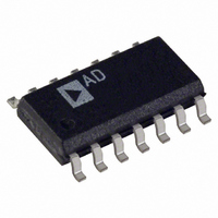
ADM489AR-REEL Analog Devices Inc, ADM489AR-REEL Datasheet

ADM489AR-REEL
Specifications of ADM489AR-REEL
Related parts for ADM489AR-REEL
ADM489AR-REEL Summary of contents
Page 1
FEATURES Meets EIA RS-485 and RS-422 standards 250 kbps data rate Single 5 V ± 10% supply − +12 V bus common-mode range 12 kΩ input impedance 2 kV EFT protection meets IEC1000-4-4 High EM immunity meets IEC1000-4-3 ...
Page 2
ADM488/ADM489 TABLE OF CONTENTS Features .............................................................................................. 1 Applications....................................................................................... 1 General Description ......................................................................... 1 Functional Block Diagrams............................................................. 1 Specifications..................................................................................... 3 Timing Specifications .................................................................. 4 Absolute Maximum Ratings............................................................ 5 ESD Caution.................................................................................. 5 Pin Configurations and Function Descriptions ........................... 6 Test Circuits................................................................................... 7 ...
Page 3
SPECIFICATIONS ± 10%. All specifications T CC MIN Table 1. Parameter DRIVER Differential Output Voltage Δ|V | for Complementary Output States OD Common-Mode Output Voltage Δ|V | for Complementary Output States OC ...
Page 4
ADM488/ADM489 TIMING SPECIFICATIONS ± 10%. All specifications T CC MIN Table 2. Parameter DRIVER Propagation Delay Input to Output, T PLH Driver O/P to OP, T SKEW Driver Rise/Fall Time Driver ...
Page 5
ABSOLUTE MAXIMUM RATINGS T = 25°C, unless otherwise noted. A Table 3. Parameter V CC Inputs Driver Input (DI) Control Inputs (DE, RE) Receiver Inputs (A, B) Outputs Driver Outputs Receiver Output Power Dissipation 8-Lead PDIP θ , Thermal Impedance ...
Page 6
ADM488/ADM489 PIN CONFIGURATIONS AND FUNCTION DESCRIPTIONS Table 4. ADM488 Pin Function Descriptions Pin No. Mnemonic Description 1 V Power Supply ± 10 Receiver Output. When A > 200 mV high. If ...
Page 7
TEST CIRCUITS V OD Figure 6. Driver Voltage Measurement Test Circuit 375Ω V 60Ω OD3 375Ω Figure 7. Driver Enable/Disable Test Circuit TST Rev Page ADM488/ADM489 A ...
Page 8
ADM488/ADM489 SWITCHING CHARACTERISTICS 3V 1.5V T PLH 0V B 1/2VO SKEW +VO 90% POINT 0V 10% POINT – Figure 11. Driver Propagation Delay, Rise/Fall Timing 0V A–B A–B T PLH RO 1.5V Figure 12. Receiver ...
Page 9
TYPICAL PERFORMANCE CHARACTERISTICS 0.5 1.0 1.5 OUTPUT VOLTAGE (V) Figure 15. Output Current vs. Receiver Output Low Voltage 0 –5 –10 –15 –20 3.4 3.6 3.8 4.0 4.2 4.4 OUTPUT ...
Page 10
ADM488/ADM489 100 500kHz/DIV Figure 21. Driver Output Waveform and FFT Plot Transmitting at 150 kHz FREQUENCY (MHz) Figure 22. Radiated Emissions ...
Page 11
THEORY OF OPERATION The ADM488/ADM489 are ruggedized RS-485 transceivers that operate from a single 5 V supply. They contain protection against radiated and conducted interference and are ideally suited for operation in electrically harsh environments or where cables can be ...
Page 12
ADM488/ADM489 V 300ms V 5ns 50ns 0.2/0.4ms Figure 25. IEC1000-4-4 Fast Transient Waveform Table 8 shows the peak voltages for each of the environments. Table 8. Peak Voltages Level V (kV) PSU PEAK 1 0 ...
Page 13
The ADM488/ADM489 comfortably meet Classification 1 at the most stringent (Level 3) requirement. In fact, field strengths V/m showed no performance degradation, and error- free data transmission continued even during irradiation. Table 9. Field Strengths Level V/m ...
Page 14
ADM488/ADM489 APPLICATION INFORMATION DIFFERENTIAL DATA TRANSMISSION Differential data transmission is used to reliably transmit data at high rates over long distances and through noisy environments. Differential transmission nullifies the effects of ground shifts and noise signals, which appear as common-mode ...
Page 15
OUTLINE DIMENSIONS 0.400 (10.16) 0.365 (9.27) 0.355 (9.02 0.280 (7.11) 0.250 (6.35) 1 0.240 (6.10) 4 PIN 1 0.100 (2.54) BSC 0.060 (1.52) 0.210 MAX (5.33) MAX 0.015 0.150 (3.81) (0.38) 0.015 (0.38) MIN 0.130 (3.30) GAUGE PLANE ...
Page 16
... ADM489AN −40°C to +85°C ADM489ANZ 1 −40°C to +85°C ADM489AR −40°C to +85°C ADM489AR-REEL −40°C to +85°C ADM489AR-REEL7 −40°C to +85°C 1 ADM489ARZ −40°C to +85°C 1 ADM489ARZ-REEL −40°C to +85°C 1 ADM489ARZ-REEL7 −40°C to +85°C ADM489ARU − ...


