MTP12P10 ON Semiconductor, MTP12P10 Datasheet

MOSFET Power 100V 12A P-Channel

MTP12P10

Manufacturer Part Number
MTP12P10
Description
MOSFET Power 100V 12A P-Channel
Manufacturer
ON Semiconductor
Datasheet

Specifications of MTP12P10

Configuration
Single
Transistor Polarity
P-Channel
Resistance Drain-source Rds (on)
0.3 Ohms
Forward Transconductance Gfs (max / Min)
2 S
Drain-source Breakdown Voltage
- 100 V
Gate-source Breakdown Voltage
+/- 20 V
Continuous Drain Current
12 A
Power Dissipation
75 W
Maximum Operating Temperature
+ 150 C
Mounting Style
Through Hole
Package / Case
TO-220AB
Minimum Operating Temperature
- 65 C
Lead Free Status / Rohs Status
No

Available stocks

Company
Part Number
Manufacturer
Quantity
Price
Part Number:
MTP12P10
Manufacturer:
ON
Quantity:
428
Part Number:
MTP12P10
Manufacturer:
ST
Quantity:
10 000
Part Number:
MTP12P10G
Manufacturer:
FSC
Quantity:
5 000
Part Number:
MTP12P10G
Manufacturer:
ON/安森美
Quantity:
20 000
MTP12P10
Power MOSFET
12 Amps, 100 Volts
P−Channel TO−220
power switching applications such as switching regulators, converters,
solenoid and relay drivers.
Features
Stresses exceeding Maximum Ratings may damage the device. Maximum
Ratings are stress ratings only. Functional operation above the Recommended
Operating Conditions is not implied. Extended exposure to stresses above the
Recommended Operating Conditions may affect device reliability.
*For additional information on our Pb−Free strategy and soldering details, please
© Semiconductor Components Industries, LLC, 2006
June, 2006 − Rev. 4
MAXIMUM RATINGS
download the ON Semiconductor Soldering and Mounting Techniques
Reference Manual, SOLDERRM/D.
Drain−Source Voltage
Drain−Gate Voltage (R
Gate−Source Voltage
Drain Current − Continuous
Drain Current
Total Power Dissipation
Derate above 25°C
Operating and Storage Temperature Range
Thermal Resistance
Maximum Lead Temperature for Soldering
Purposes, 1/8″ from case for 10 seconds
This Power MOSFET is designed for medium voltage, high speed
at 100°C
at Elevated Temperature
Silicon Gate for Fast Switching Speeds − Switching Times Specified
Designer’s Data − I
Rugged − SOA is Power Dissipation Limited
Source−to−Drain Diode Characterized for Use With Inductive Loads
Pb−Free Package is Available*
− Continuous
− Non−repetitive (t
− Junction−to−Case
Junction−to−Ambient°
− Pulsed
Rating
GS
DSS
(T
= 1.0 MW)
C
, V
p
= 25°C unless otherwise noted)
Preferred Device
≤ 50 ms)
DS(on)
, V
GS(th)
Symbol
T
V
V
V
R
R
and SOA Specified
J
V
I
DGR
GSM
P
, T
DSS
DM
T
I
qJC
qJA
GS
D
D
L
stg
−65 to 150
Value
1.67
62.5
100
100
± 20
± 40
260
0.6
12
28
75
1
W/°C
°C/W
Unit
Vdc
Vdc
Vdc
Vpk
Adc
°C
°C
W
MTP12P10
MTP12P10G
Preferred devices are recommended choices for future use
and best overall value.
1
2
Device
3
12 AMPERES, 100 VOLTS
MTP12P10 = Device Code
A
Y
WW
G
ORDERING INFORMATION
4
R
G
CASE 221A
DS(on)
TO−220AB
http://onsemi.com
STYLE 5
TO−220AB
TO−220AB
(Pb−Free)
Package
P−Channel
= Location Code
= Year
= Work Week
= Pb−Free Package
D
AND PIN ASSIGNMENT
= 300 mW
Publication Order Number:
MARKING DIAGRAM
Gate
S
1
MTP12P10G
AYWW
Drain
Drain
4
2
50 Units/Rail
50 Units/Rail
Shipping
MTP12P10/D
3
Source

Related parts for MTP12P10

MTP12P10 Summary of contents

Page 1

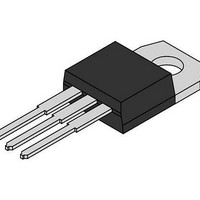
... MARKING DIAGRAM AND PIN ASSIGNMENT 4 Drain 4 TO−220AB CASE 221A MTP12P10G STYLE 5 AYWW Gate 2 Drain MTP12P10 = Device Code A = Location Code Y = Year WW = Work Week G = Pb−Free Package ORDERING INFORMATION Device Package Shipping MTP12P10 TO−220AB 50 Units/Rail MTP12P10G TO−220AB 50 Units/Rail (Pb−Free) Preferred devices are recommended choices for future use and best overall value ...

Page 2

... Internal Source Inductance (Measured from the source lead 0.25″ from package to source bond pad) 1. Pulse Test: Pulse Width ≤ 300 ms, Duty Cycle ≤ 2%. MTP12P10 (T = 25°C unless otherwise noted ...

Page 3

... V , GATE−TO−SOURCE VOLTAGE (VOLTS) GS Figure 3. Transfer Characteristics 0 100°C J 0.4 0.3 25°C 0.2 −55°C 0 DRAIN CURRENT (AMPS) D Figure 5. On−Resistance versus Drain Current MTP12P10 1 −50 −25 Figure 2. Gate−Threshold Voltage Variation 1 0. 1 −50 −75 Figure 4. Normalized Breakdown Voltage 1 ...

Page 4

... The power averaged over a complete switching cycle must be less than: P (pk DUTY CYCLE 0 TIME (ms) Figure 9. Thermal Response http://onsemi.com 4 MTM/MTP12P06 MTM/MTP12P10 DRAIN−TO−SOURCE VOLTAGE (VOLTS) DS Figure 8. Maximum Rated Switching Safe Operating Area and the breakdown voltage − T J(max) C ...

Page 5

... C iss 800 C oss 400 C rss SOURCE−TO−DRAIN VOLTAGE (VOLTS) DS Figure 10. Capacitance Variation V in PULSE GENERATOR gen Figure 12. Switching Test Circuit MTP12P10 0 − 25° − MHz −6 −8 −10 −12 −14 − Figure 11. Gate Charge versus RESISTIVE SWITCHING d(on) ...

Page 6

... V 0.045 −−− 1.15 −−− Z −−− 0.080 −−− 2.04 STYLE 5: PIN 1. GATE 2. DRAIN 3. SOURCE 4. DRAIN ON Semiconductor Website: www.onsemi.com Order Literature: http://www.onsemi.com/orderlit For additional information, please contact your local Sales Representative MTP12P10/D ...

Related keywords