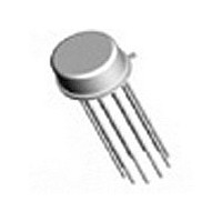
JM38510/10306BIA National Semiconductor, JM38510/10306BIA Datasheet - Page 5

JM38510/10306BIA
Manufacturer Part Number
JM38510/10306BIA
Description
Manufacturer
National Semiconductor
Datasheet
1.JM3851010306BIA.pdf
(12 pages)
Specifications of JM38510/10306BIA
Number Of Elements
2
Output Type
Open Collector
Technology
Bipolar
Input Offset Voltage
4@±15VmV
Single Supply Voltage (typ)
9/12/15/18/24/28V
Dual Supply Voltage (typ)
±3/±5/±9/±12/±15V
Supply Current (max)
10@±15VmA
Power Supply Requirement
Single/Dual
Common Mode Rejection Ratio
90dB
Voltage Gain In Db
80dB
Single Supply Voltage (min)
5V
Single Supply Voltage (max)
36V
Dual Supply Voltage (min)
±2.5V
Dual Supply Voltage (max)
±18V
Power Dissipation
500mW
Operating Temp Range
-55C to 125C
Operating Temperature Classification
Military
Mounting
Through Hole
Pin Count
10
Package Type
TO-100
Lead Free Status / Rohs Status
Not Compliant
tR
tR
V
±I
IO
Symbol
Symbol
IB
AC Parameters
The following conditions apply to all the following parameters, unless otherwise specified.
AC: ±15V, C
LHC
HLC
DC Drift Parameters
Delta calculations performed at Group B-5
Note 1: Absolute Maximum Ratings indicate limits beyond which damage to the device may occur. Operating Ratings indicate conditions for which the device is
functional, but do not guarantee specific performance limits. For guaranteed specifications and test conditions, see the Electrical Characteristics. The guaranteed
specifications apply only for the test conditions listed. Some performance characteristics may degrade when the device is not operated under the listed test
conditions.
Note 2: The maximum power dissipation must be derated at elevated temperatures and is dictated by T
junction to ambient thermal resistance), and T
θ
Note 3: For supply voltages less than ±15V the absolute maximum input voltage is equal to the supply voltage.
Note 4: Human Body model, 1.5KΩ in series with 100pF.
Note 5: K = V/mV.
JA
or the number given in the Absolute Maximum Ratings, whichever is lower.
Response Time (Collector
Output)
Response Time (Collector
Output)
Input Offset Voltage
Input Bias Current
L
= 50pF
Parameter
Parameter
201481 Version 2 Revision 3
A
(ambient temperature). The maximum allowable power dissipation at any temperature is P
V
V
V
V
+V
V
+V
V
+V
V
+V
V
+V
V
+V
V
OD
I
OD
I
CM
CM
CM
CM
CM
CM
= 100mV
= 100mV
CC
CC
CC
CC
CC
CC
(overdrive) = +5mV,
(overdrive) = -5mV,
= 0V, R
= -12V, R
= 12V, R
= 0V
= -12V
= 12V
= 15V, -V
= 27V, -V
= 3V, -V
= 15V, -V
= 27V, -V
= 3V, -V
Conditions
Conditions
S
S
= 50Ω
CC
CC
S
= 50Ω
CC
CC
CC
CC
= 50Ω
= -27V,
= -27V,
Print Date/Time: 2010/09/30 23:38:32
= -15V,
= -3V,
= -15V,
= -3V,
5
Notes
Notes
Jmax
(maximum junction temperature), θ
Min
Min
-1.0
-1.0
-1.0
-50
-50
-50
Max
Max
125
160
1.0
1.0
1.0
50
50
50
Unit
Unit
mV
mV
mV
nS
nS
nA
nA
nA
Dmax
= (T
JA
www.national.com
(package
Jmax
groups
groups
- T
Sub-
Sub-
9
9
1
1
1
1
1
1
A
)/


